Croatian
 Bulgarian
 Chinese (Traditional)
 Arabic
 Sindhi
 Shona
Shona Scottish Gaelic
 Samoan
 Pashto
 Luxembourgish
 Kyrgyz
 Kurdish (Kurmanji)
 Hawaiian
 Corsican
 Amharic
 Uzbek
Uzbek Tajik
Tajik Sundanese
 Sesotho
 Sinhala
 Malayalam
 Malagasy
 Kazakh
 Chichewa
 Myanmar (Burmese)
 Zulu
Zulu Yoruba
 Telugu
 Tamil
Tamil Somali
 Punjabi
 Nepali
 Mongolian
 Marathi
 Maori
Maori Latin
Latin Lao
Lao Khmer
Khmer Kannada
 Javanese
 Igbo
Igbo Hmong
Hmong Hausa
Hausa Esperanto
 Cebuano
 Bosnian
 Bengali
 Urdu
Urdu Haitian Creole
 Georgian
 Basque
 Azerbaijani
 Armenian
 Yiddish
 Macedonian
 Icelandic
 Belarusian
 Welsh
Welsh Irish
Irish Swahili
 Malay
Malay Afrikaans
 Persian
 Turkish
 Thai
Thai Maltese
 Hungarian
 Galician
 Estonian
 Albanian
 Vietnamese
 Ukrainian
 Slovenian
 Slovak
 Serbian
 Lithuanian
 Latvian
 Indonesian
 Hebrew
 Filipino
 Catalan
 Swedish
 Spanish
 Russian
 Romanian
 Portuguese
 Polish
 Norwegian
 Korean
 Japanese
 Italian
 Hindi
Hindi Greek
Greek German
 French
 Finnish
 Czech
Czech Danish
 Dutch
DutchService hotline
+86 0755-83975897
 en
en 
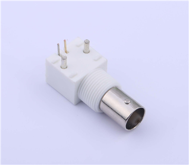
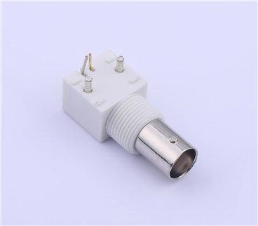
Release date:2025-02-19Author source:KinghelmViews:1369
The traditional CPW features a G-S-G configuration, where the signal line and grounds are situated on the same plane. In contrast, CPWG builds upon the traditional CPW by adding a ground plane on the underside of the dielectric substrate and connecting this ground plane to the top-side ground through vias.
The characteristics of CPWG encompass those of the traditional CPW, with additional benefits stemming from the inclusion of the bottom ground plane and the via connections. For the purpose of this discussion, we will focus solely on the analysis of CPWG.
From its structural perspective, the G-S-G configuration of the coplanar waveguide inherently mitigates crosstalk between signals. It also provides superior isolation and EMI performance for the traces, enabling the achievement of lower impedance.
In terms of radiation characteristics, the addition of vias introduces discontinuities, leading to impedance variations and increased losses due to these discontinuities.
When designing for millimeter-wave frequencies, with the same dielectric substrate, CPWG exhibits lower surface wave leakage and radiation losses compared to microstrip lines.
Furthermore, CPWG stands out for its superior thermal dissipation properties when used in power device applications, compared to traditional CPW.
In the design process, the following general experiences are typically applied:
1. The signal line should be enclosed by ground planes on the same layer, with a constant distance maintained to avoid discontinuities that could lead to impedance variations.
2. The distance from the signal line to the ground plane on the same layer should be maintained at the thickness of the dielectric substrate.
3. The horizontal distance between vias is generally set to λ/20 to 2mm, where λ represents the wavelength.
4. The width of the ground enclosure should be greater than the distance between the signal line and the ground planes.
5. Typically, the width of the microstrip line is designed first and then incorporated into the coplanar waveguide calculations.
1. Selecting suitable materials is crucial. For microstrip lines, the electromagnetic field is concentrated between the dielectric substrates, with strong edge effects.
2. When it comes to CPWG , using a thicker copper layer can result in enhanced electromagnetic fields between the top grounding terminals, the signal line, and the grounding field paths. Additionally, thicker copper layers in GCPW circuits can lead to the formation of more electromagnetic fields in the air above the circuit. This increased electromagnetic field in the air above the circuit can reduce both the signal loss and the effective dielectric constant loss in GCPW circuits, primarily due to the thicker copper plating layer on the PCB.
Copyright © Shenzhen Kinghelm Electronics Co., Ltd. all rights reservedYue ICP Bei No. 17113853