Croatian
 Bulgarian
 Chinese (Traditional)
 Arabic
 Sindhi
 Shona
Shona Scottish Gaelic
 Samoan
 Pashto
 Luxembourgish
 Kyrgyz
 Kurdish (Kurmanji)
 Hawaiian
 Corsican
 Amharic
 Uzbek
Uzbek Tajik
Tajik Sundanese
 Sesotho
 Sinhala
 Malayalam
 Malagasy
 Kazakh
 Chichewa
 Myanmar (Burmese)
 Zulu
Zulu Yoruba
 Telugu
 Tamil
Tamil Somali
 Punjabi
 Nepali
 Mongolian
 Marathi
 Maori
Maori Latin
Latin Lao
Lao Khmer
Khmer Kannada
 Javanese
 Igbo
Igbo Hmong
Hmong Hausa
Hausa Esperanto
 Cebuano
 Bosnian
 Bengali
 Urdu
Urdu Haitian Creole
 Georgian
 Basque
 Azerbaijani
 Armenian
 Yiddish
 Macedonian
 Icelandic
 Belarusian
 Welsh
Welsh Irish
Irish Swahili
 Malay
Malay Afrikaans
 Persian
 Turkish
 Thai
Thai Maltese
 Hungarian
 Galician
 Estonian
 Albanian
 Vietnamese
 Ukrainian
 Slovenian
 Slovak
 Serbian
 Lithuanian
 Latvian
 Indonesian
 Hebrew
 Filipino
 Catalan
 Swedish
 Spanish
 Russian
 Romanian
 Portuguese
 Polish
 Norwegian
 Korean
 Japanese
 Italian
 Hindi
Hindi Greek
Greek German
 French
 Finnish
 Czech
Czech Danish
 Dutch
DutchService hotline
+86 0755-83975897
 en
en 
Release date:2025-02-19Author source:KinghelmViews:1145
As a PCB engineer, you understand the importance of precise routing to ensure optimal performance and minimize interference. Here are some key guidelines to enhance your design process:
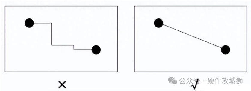
1. Keep Signal Trace Lengths Short
Shorter traces reduce unwanted interference. For critical signals like clock traces, place your oscillator close to the component to maintain signal integrity.
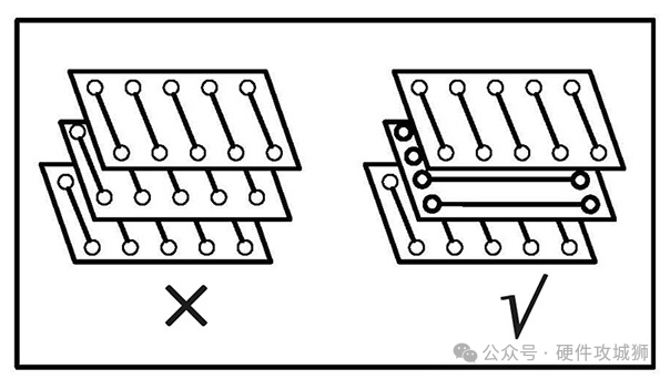
2. Control Routing Direction
Use orthogonal routing for traces on adjacent layers to prevent cross-talk. This simple technique helps maintain signal clarity across your design.
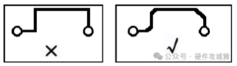
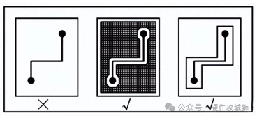
3. Avoid Sharp Corners
Right angles and sharp corners on traces can cause radiation, leading to poor performance. Round off sharp corners to improve your design's electromagnetic characteristics.
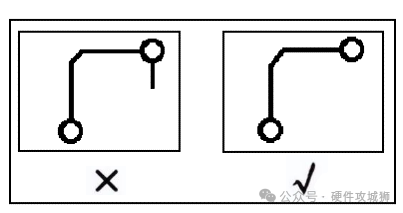
4. Minimize Open Loops
Floating traces act like antennas, picking up interference. Ensure all traces are properly connected to prevent unwanted radiation.
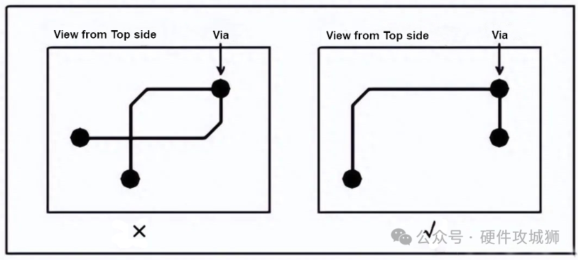
5. Watch for Self-Looping Traces
In multi-layer designs, be mindful of self-loops. Traces that loop back can introduce interference, impacting the overall signal integrity.
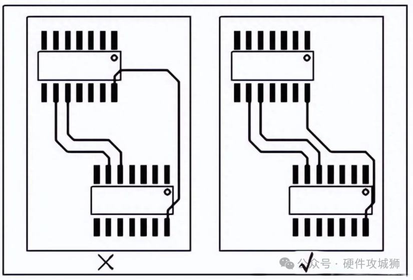
6. Reduce Ground Loop Areas
Keep the loop between signal traces and their return path as small as possible to minimize radiation and susceptibility to external noise.
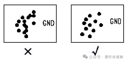
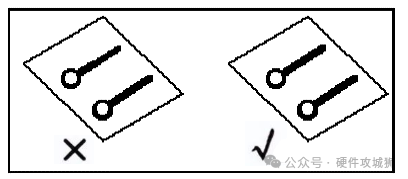
7. Maintain Power and Ground Plane Integrity
Ensure that vias do not create gaps in your power or ground planes. Maintaining a solid plane is crucial for signal performance and reliability.
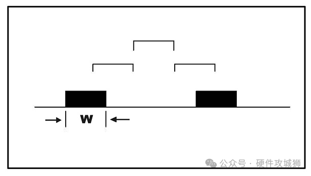
8. Follow the 3W Rule for Trace Spacing
To minimize crosstalk, space traces at least three times the width of the trace itself. For better isolation, use wider spacing.
9. Shield Sensitive Signals
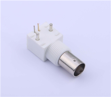
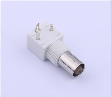
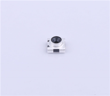
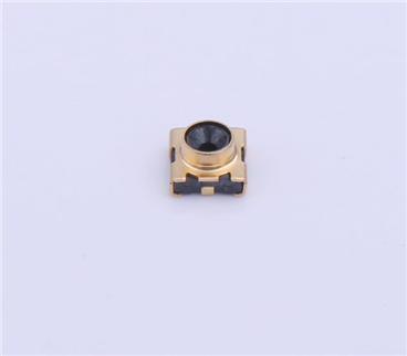
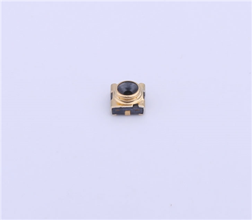
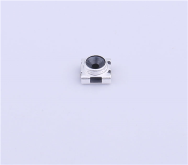
For high-frequency signals like clocks, consider shielding them with grounded traces to prevent interference. Kinghelm offers a range of components ideal for shielding-sensitive applications.
10. Ensure Impedance Matching
Consistent trace widths are key to preventing signal reflections, especially in high-speed designs. When width changes are necessary, minimize their length to maintain signal integrity.
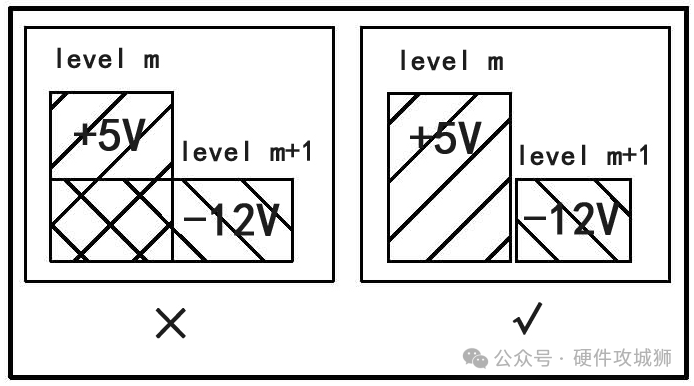
11. Avoid Overlapping Power Layers
Keep power planes separated to avoid interference between voltage domains. If overlap is unavoidable, consider inserting a ground plane in between to reduce noise.
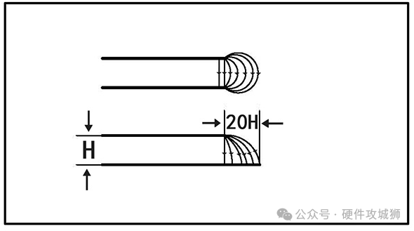
12. Apply the 20H Principle
Minimize edge radiation by pulling back the power plane by at least 20 times the dielectric thickness. This keeps most of the electric field within the ground plane, improving overall performance.
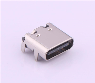
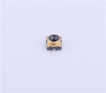
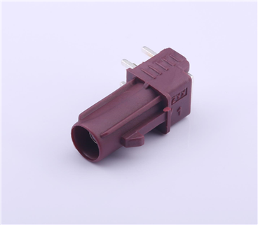
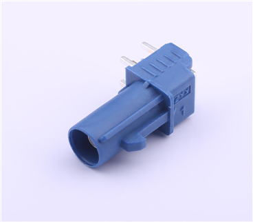
At Kinghelm, we provide a range of high-quality connectors and electronic components designed to support your PCB designs from start to finish. Whether you're designing a complex multi-layer board or a simple prototype, our components help ensure your designs meet the highest standards of performance and reliability.
Explore our website today to discover the perfect components for your next project.
Copyright © Shenzhen Kinghelm Electronics Co., Ltd. all rights reservedYue ICP Bei No. 17113853