Service hotline
+86 0755-83975897
 en
en Release date:2021-12-28Author source:KinghelmViews:2391
The introduction of USB power transmission (PD) greatly improves the power capability of USB interface protocol and has the potential to support up to 100W system. With the transmission of data, only one cable is needed to provide more power for electronic / electrical equipment. Therefore, the space used and the installation cost can be reduced. USB PD means that the power direction is no longer fixed. Therefore, depending on the specific situation, the device can act as a receiver (obtain power from VBUS) or a power supply (provide power through VBUS). The device can use PD specification to implement high-power applications and enumerate the connected hardware. After that, they can provide the necessary strength. The charging through device is an example.
Design goal
There are many potential ways to design charging through devices. The principle is that the power supply of the charger is transmitted to port 1 through port 2 to charge the connected hardware (such as laptop). However, this can be achieved in many different ways, and each has its specific advantages and disadvantages.
Obtain vsafe5v
In this section, we will introduce two different design methods that can be used for vsafe5v implementation. In one design, vsafe5v also passes through port 2, while in another design, vsafe5v is internally generated.
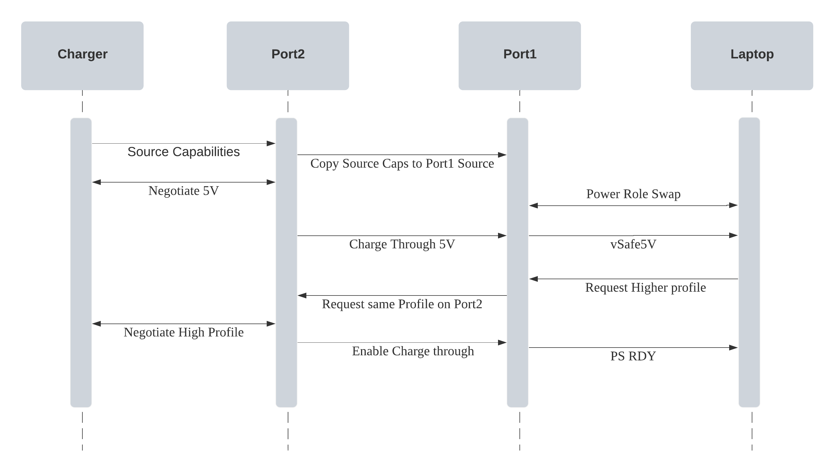
Figure 1: schematic diagram describing the implementation of vsafe5v charging through port 2
The vsafe5v passing through port 2 is described in Figure 1. When the connected hardware requests a higher power profile, port 2 will negotiate the same profile. Once port 2 completes the negotiation process, port 1 will notify the laptop that power is ready.
The main advantage of this method is that it keeps the design simple and does not need to use an internal 5V generator. However, this route also has some disadvantages. Since vsafe5v is straight through, the voltage level and current capacity will depend directly on the port 2 power supply. If the input voltage is close to the lower limit of PD specification (4.75V to 5.5V), vsafe5v may be lower than the specification on port 1 side. This is caused by the voltage drop through the circuit. Another disadvantage to note is that the high voltage negotiation process must undergo additional negotiation steps on the port 2 side. This may be a bit time-consuming, so it is possible to exceed the PD timing specification.
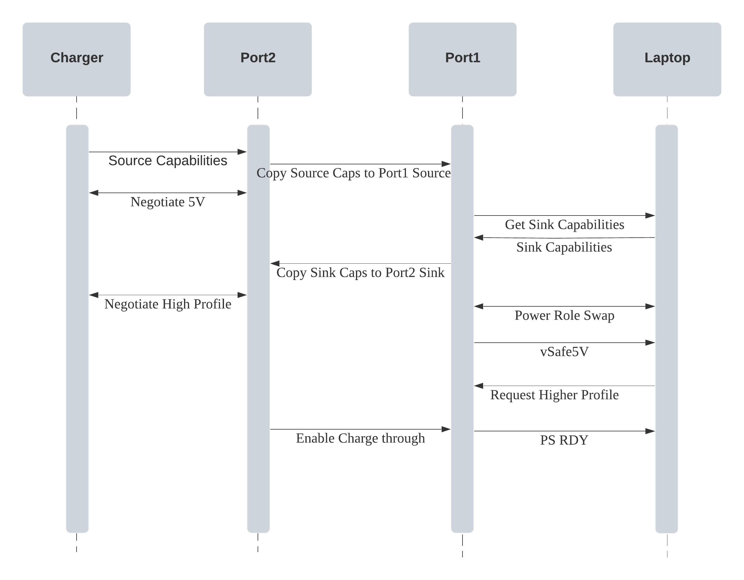
Figure 2: schematic diagram of on-board vsafe5v straight through implementation
Another option available is to generate vsafe5v on the palette, as shown in Figure 2. In this case, vsafe5v can be generated in full compliance with the usbpd specification. The example shown here uses the receiver function of the laptop and determines the best charging mode for the connected device. Then negotiate the profile through port 2 and set the voltage level before the role switches to port 1. Once the switch to port 1 is complete, it can set a higher profile for the connection hardware request because the charging profile is already available on port 2.
This design layout is advantageous because the performance of vsafe5v can be predicted. The reason is that vsafe5v is generated internally. In addition, the negotiation voltage does not have to be renegotiated on port 2, which will speed up the turnaround time experienced. However, this approach has an obvious disadvantage that needs to be recognized. This type of design cannot be used for certain hosts, that is, hosts that switch between multiple profiles. Based on the various hosts and hubs tested by the ftdi engineering team, differences in the implementation of power negotiation were observed among different manufacturers.
Other considerations
In addition to the vsafe5v detailed above, other factors need to be considered when designing the charging through device. These include:
1. VBUS discharge - since the direct charging device will initially act as a receiver, the engineer must be aware of the need for VBUS discharge. When a device is disconnected as a source, it needs to return to its original role as a receiver. At the same time, VBUS must discharge across the whole passage path within the specified time period.
2. Voltage drop - the voltage drop across the entire pass through path must be minimized.
In order to ensure that the power path in the partial discharge system operates in an effective way, a load switch controlled by the through partial discharge device is used. This load switch will include a pass transistor (usually a MOSFET with an on / off control block). Since the charging current of partial discharge can be as high as 5a, it must be remembered that the drain source on resistance (RDSON) in the load switch must be low, so that the power loss involved will not be too large, and the voltage at port 1 remains within the partial discharge specification.
3. Surge current limit - when the charger is connected to port 2 and the charging device is connected to port 1, surge current may be generated if the capacitive load is switched to the power rail. The magnitude of surge current will depend on the rise time of voltage rise and load capacitance. A steep voltage ramp will increase the surge current and cause a transient drop in VBUS. This may cause the connected hardware to reset itself, which needs to be avoided. In addition to affecting the function of the connecting hardware, this condition may damage or shorten the service life of the load switch assembly. Although large load capacitance will reduce the transient voltage drop, it will increase the inrush current. Therefore, it is necessary to control the conversion rate of the load switch to prolong the rise time of the voltage ramp, and optimize the load capacitance to limit the inrush current and drop in VBUS. Another advantage of switching rate control on the load switch is that as an overcurrent protection measure (due to the presence of high surge current), it can prevent the charger from turning off the power supply of the through device, because this will obviously lead to the interruption of partial discharge charging.
4. Internal power consumption - for the purpose of internal power consumption, it is obvious that a certain amount of power needs to be deducted from the charging mode. This needs to be taken into account when determining the operating parameters of the system.
Conclusion
The overall design goal of PD equipment with direct connection capability is to ensure smooth connection and power supply between various USB PD hosts or hubs. If engineers ensure that they fully understand all the projects discussed in this article, they will be able to achieve this goal. Ftdi provides the advanced dual port IC technology required to support the development of USB power transmission system, as described above. The company's power transmission IC allows hardware to switch from a receiver to a source without any data flow interruption.
This content comes from the network / electronic innovation network. This website only provides reprint. The views, positions and technologies of this article have nothing to do with this website. If there is infringement, please contact us to delete it!
Copyright © Shenzhen Kinghelm Electronics Co., Ltd. all rights reservedYue ICP Bei No. 17113853
