Service hotline
+86 0755-83975897
Release date:2021-12-28Author source:KinghelmViews:3037
In recent years, mobile communication has been rapidly developed and popularized in China, and the transmitter and receiver technology of wireless communication has also developed rapidly. The main function of RF transmitter is to realize baseband signal modulation, up conversion and power amplification. Compared with the structure of the receiver, the structure of the transmitter is relatively simple. Usually:
· Direct up conversion (also known as zero if modulation)
· Indirect up conversion (also known as two-stage frequency conversion or superheterodyne type)
· Digital IF transmitter
The structure of standard IQ quadrature modulation circuit is very simple. It is divided into IQ baseband generator and IQ mixer. Whether it is amplitude modulation, frequency modulation or phase modulation, it can be realized only by changing different IQ baseband signals. The function of IQ modulator is to move the baseband IQ signal to the carrier. Quadrature modulator can usually achieve high phase accuracy and amplitude balance, and is very suitable for direct up conversion (zero if modulation) in communication system. Therefore, it is widely used in direct up conversion transmitters, such as cellular mobile communication, WLAN, UWB super communication system, Bluetooth, GPS and other systems. It is a key element in modern wireless communication system.
The block diagram of quadrature modulator is shown in Figure 1 below. If it is used for direct up conversion transmitter, the second LO, if filter and mixer are omitted, which simplifies the transmitter system structure, thus reducing the cost, volume and power consumption.
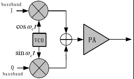
Figure 1 Principle block diagram of quadrature modulator
The inherent disadvantages of quadrature modulator are LO leakage and sideband suppression (LO leakage is mainly caused by DC bias of IQ signal, imbalance of IQ differential signal and poor isolation index of lo and RF). Ideally, the quadrature modulator only moves and superimposes the baseband spectrum, and will not cause the out of band spectrum proliferation or in band distortion of the signal. The quadrature modulator will inevitably have non ideal factors, resulting in various distortion of the output signal and affecting the communication quality, so the RF performance of the quadrature modulator needs to be tested in all aspects.
The single sideband CW signal is generally used to test the image suppression of IQ modulator, and the input I signal is sin ω 0t, Q signal: cos ω 0t is mixed with the orthogonal local oscillator to obtain the modulation signal s (T), where ω 0 is generally a sweep signal, starting from near DC to tens or hundreds of megabytes:
s(t)=sinω0t∙cosωct-cosω0t∙ sinωc t
=sin(ωc-ω0 )t
If the IQ modulator is completely ideal, it will only( ω c- ω 0) generates a single sideband signal (single sideband CW signal), but due to the non ideality of the modulator, it will also( ω c+ ω A mirror signal is generated at 0). At the same time, at the local oscillator frequency ω C position will also have a signal called LO leakage. The suppression of local oscillator and mirror signal is an important index of IQ modulator. Fig. 2 is the single sideband CW output result of a typical IQ modulator. The carrier is 10g, the IQ signal is 30MHz, and the rejection of the mirror signal is 42db. At this time, the arbitrary waveform generator is used to generate two channels of 30MHz sin and COS signals, which are respectively provided to the IQ modulator as the baseband input. The two channels of the vector network with dual source option can also be used to output CW continuous waves with a constant phase difference of 90 degrees. Another advantage of using the vector network is that the local oscillator and image suppression system can be tested in the sweep mode.
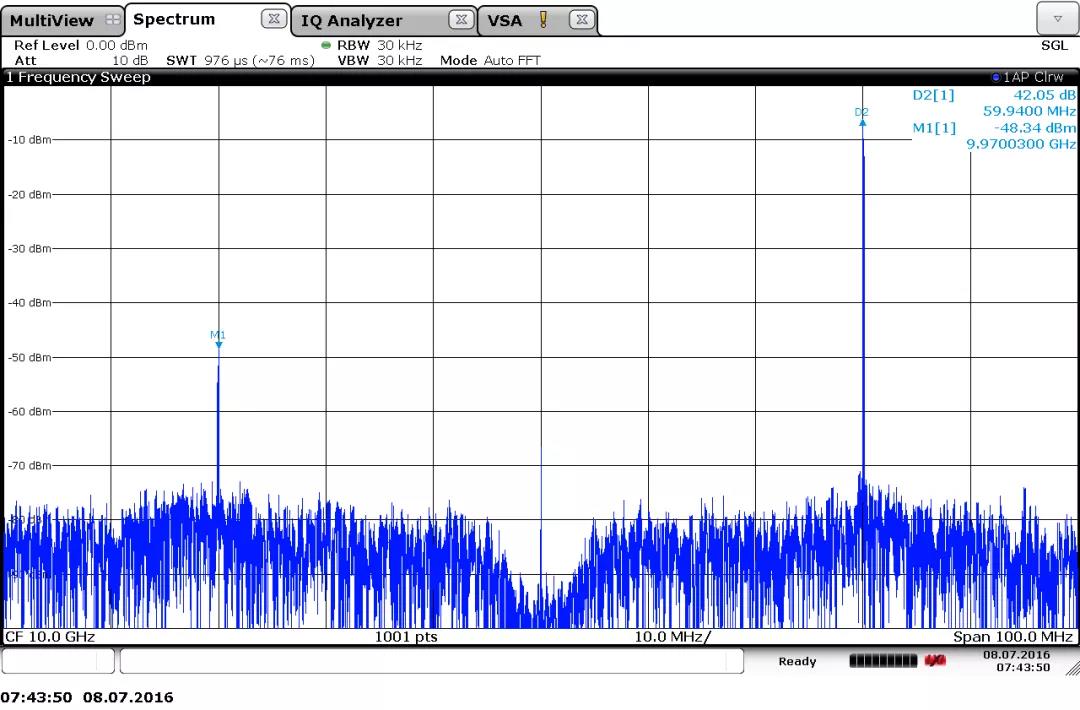
Figure 2 The spectrum analyzer tests the IQ modulation of vector signal source
2. Test task
The quadrature modulator used in this paper is adl5371 from analog devices. Its working frequency range is 500 MHz ~ 1.5 GHz. As shown in Figure 3 below, I +, I -, q + and q-ports of the device are IQ dual differential baseband input respectively, and lo is single ended Lo input (loin is connected to matching load). The baseband input requires a bias voltage of 500mv. The RF output Vout is single ended 50 Ω.
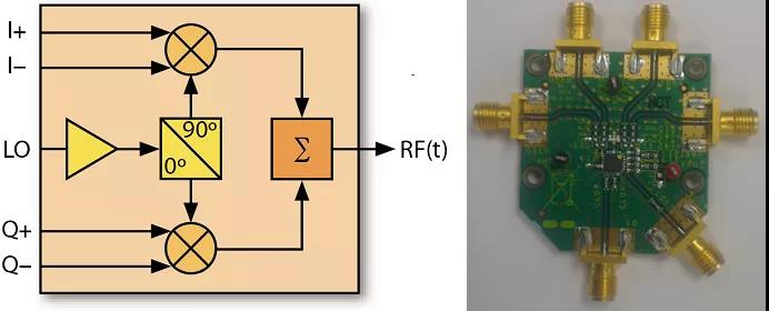
Figure 3 Quadrature modulator adl5371 pin (left) and adl5371 evaluation board
During the test, the evaluation board of adl5371 needs to input a single ended lo of 0dbm and 900MHz. The peak to peak value of the sine wave of IQ dual differential baseband input is 1.4V, the frequency is 1MHz, and has a 500mv bias voltage. Test items include: output power; Output 1dB compression point; Carrier feedthrough; Sideband suppression; Quadrature phase error; IQ amplitude imbalance; Second and third harmonic suppression; TOI; Baseband to RF amplitude frequency response.
3. Test platform
The core of the test platform is vector signal source and signal and spectrum analyzer, as shown in the figure below. It also includes DC power supply and multimeter (voltage measurement). Adl5371 is installed on the evaluation board Q mod. The vector signal source is usually equipped with differential IQ output, which can output the baseband IQ in the form of differential signal from the four BNC connectors on the rear panel.
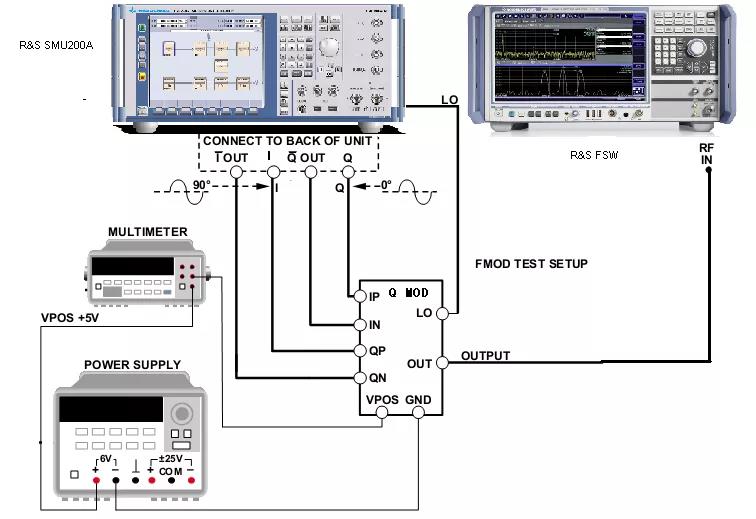
Figure 4 Quadrature modulator test platform
4. Test result
4.1 Basic setting of signal source
The signal source settings of the test items in 4.2 ~ 4.4 are shown in the figure below. The baseband generates 1MHz sine wave, the baseband IQ output adopts differential mode, the peak output voltage is 0.7V, and the IQ port bias voltage is 500mv.
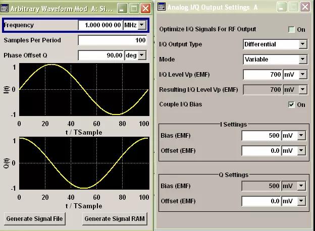
Figure 5 Basic setting of signal source smu200a
4.2 Output power
As can be seen from the mark M1 in Figure 6, the output power is 7.86dbm
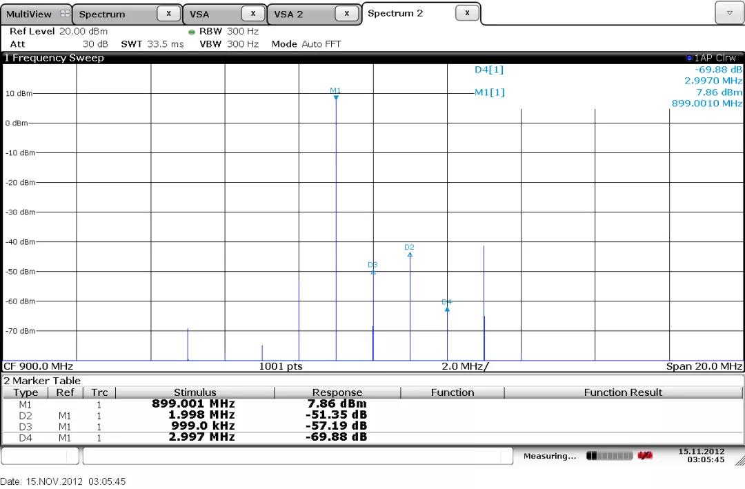
Figure 6 Output power test results
4.3 Local oscillator leakage and sideband suppression, second and third harmonics
It can be seen from D3 and D2 in Figure 7 that the sideband suppression is - 51.5dbc and the LO leakage is - 57dbc
According to D4 and D1 in Figure 7, the second harmonic suppression degree is - 72db and the third harmonic suppression system is - 53db.
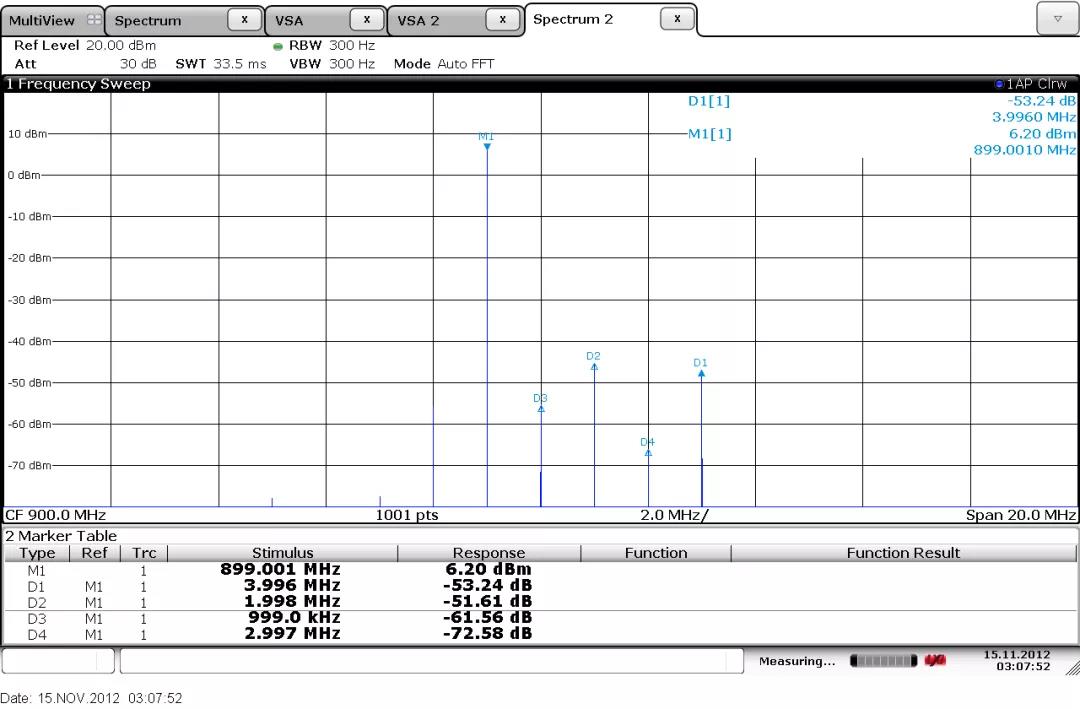
Figure 7 Output power test results, local oscillator leakage and sideband suppression, second harmonic and third harmonic measurement results
4.4 1dB compression point
Increase the differential IQ output voltage in 1dB steps. When the increased value of output power is less than 1dB on the spectrometer, the 1dB compression point is measured. As shown in Figure 8 below, the output compression point is 13.8dbm, and the corresponding input IQ power read on the signal source is 1.567v.
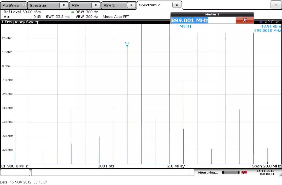
Figure 8 1dB compression point measurement results
4.5 IQ amplitude imbalance and quadrature phase error
The signal source generates QPSK with 1m symbol rate, and the setting of IQ output is the same as the previous test items. Using the vector signal analysis (VSA) demodulation of the spectrometer, the test results in Figure 9 below show that the quadrature phase error is 0.08 degrees and the IQ amplitude imbalance is 0.04db.
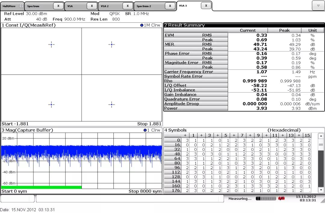
Figure 9 IQ unsatisfactory characteristic measurement results
4.6 TOI
The standard multi carrier function of the signal source generates 3.5MHz and 4.5mhz dual tone IQ signals. The IQ output setting is the same as the previous test items. Adjust the IQ input voltage until the dual tone signal output power reaches 1.6dbm. Using the toi function of the spectrometer, the measured toi is 27.7dbm.
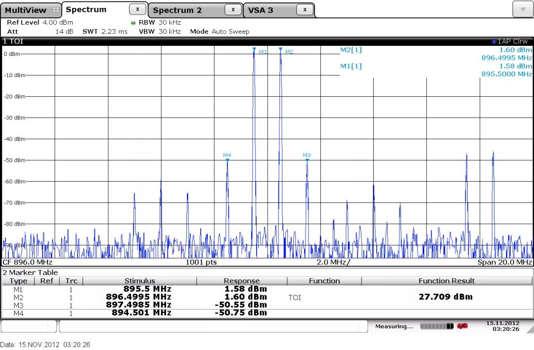
Figure 10 Toi measurement results
4.7 Baseband to RF amplitude frequency response
For the amplitude frequency response test, the baseband frequency offset needs to be changed step by step by computer program-controlled signal source, and the measurement trace of the spectrometer adopts the maximum holding function. As can be seen from Fig. 11, from 900MHz to 940mhz, the maximum amplitude frequency response of the quadrature modulator evaluation board is 7.8dbm and the minimum value is 7.1dbm. It should be noted that the above amplitude frequency response measurement results are the measurement results of the adl5371 evaluation board. If you want to obtain the 1dB and 0.1dB bandwidth of the adl5371 chip, you need to calibrate and correct the circuit characteristics of the evaluation board circuit.
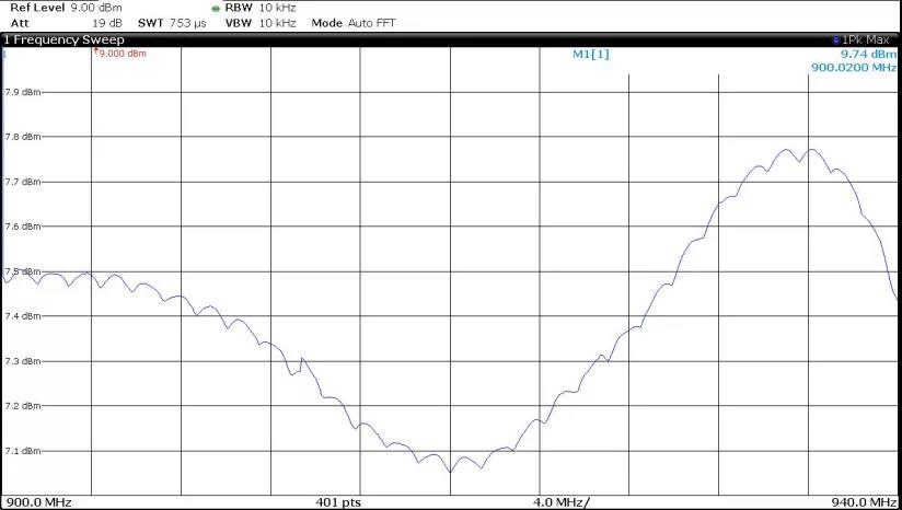
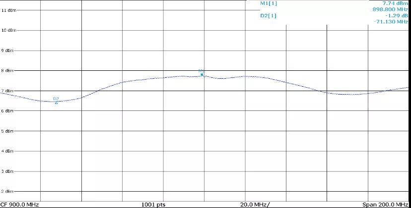
Figure 11 The amplitude frequency response measurement results are measured by smu200a (upper) and afq100b (lower)
This content comes from the network / microwave RF network. This website only provides reprint. The views, positions and technologies of this article have nothing to do with this website. If there is infringement, please contact us to delete it!
Copyright © Shenzhen Kinghelm Electronics Co., Ltd. all rights reservedYue ICP Bei No. 17113853