Service hotline
+86 0755-83975897
Release date:2021-12-28Author source:KinghelmViews:2194
The three-dimensional heterogeneous integration technology of micro system is the most promising technology to realize the requirements of higher integration, higher performance and higher working frequency of RF electronic system in the future. This paper analyzes the application requirements and prospects of RF micro system integration technology in military and civilian fields, and systematically summarizes its technical connotation and technical system, The new challenges and solutions of Microsystem integration technology in design simulation, thermal management, testing, process and reliability are explained, and the further development ideas of RF microsystem integration technology are put forward.

Moore's law is close to the physical limit, but the electronic information system will continue to develop towards higher integration, higher performance and higher working frequency in the future. The traditional integrated packaging technology is gradually difficult to meet the requirements of new system integration. The future technology development trend will be to continue Moore's law and surpass Moore's law, and realize a higher value system - microsystem through three-dimensional heterogeneous integration. Microsystem integration technology is the main means to achieve higher integration, higher performance and higher working frequency by using heterogeneous and heterogeneous integration methods on micro and nano scale. As an advanced integrated packaging technology under the trend of system miniaturization, RF microsystem integration technology has become a major basic technology to lead equipment development and promote electronic technology innovation. It is an important technical platform to support the capability transformation of electronic information equipment in the fields of sensing and communication. At the same time, it is also one of the core technologies of current electronic information technology research.
This paper analyzes the application requirements and prospects of RF micro system integration technology in military and civil fields, systematically summarizes its technical connotation, combs out the system framework of micro system integration technology in three aspects: design simulation, process integration and test verification, and studies and judges the challenges and development opportunities faced by the technology, At the same time, the further development ideas of RF microsystem integration technology are put forward.
1 overview of RF micro system micro integration technology
1.1 application of RF microsystem integration technology in military and civilian market

In the military field, the future intelligent combat requirements of weapons and equipment will rely more on highly integrated electronic information systems. The development of new generation radar, communication, electronic warfare and other cutting-edge weapons and equipment puts forward an urgent demand for RF microsystem integration. RF micro system integration can realize the high integration of functional modules or subsystems based on new ideas and new processes on the micro and nano scale, and then realize the characteristics of greatly reducing the volume and power consumption of weapons and equipment, greatly improving the performance and reliability, greatly reducing the channel cost and life cycle cost, supporting multi-function and gradually becoming intelligent.
In the civil field, 5g / 6G communication, Internet of things, unmanned driving, terahertz imaging, biomedicine and other fields all put forward a wide range of application requirements for RF microsystem integration. Through silicon via (TSV) technology, through glass via (TGV) technology, wafer level packaging (WLP) technology, three-dimensional stacking and other three-dimensional heterogeneous integration technologies integrate front-end RF transceiver devices, data processor devices, high-frequency storage devices and efficient power supply, which can greatly improve the functions of products and reduce the delay of device interconnection and the mismatch between RF transmission, Realize the high-frequency, broadband and high-speed transmission of signals, so as to effectively reduce the power consumption and volume of products. Figure 2 shows the 5g RF micro system implemented by Ericsson and IBM, which realizes the high-density integrated integration of 64 channel antenna array. Figure 3 , shows the research results of automotive radar released by A-star Research Institute in Singapore. It uses TSV technology combined with novel embedded wafer level packaging technology to produce a 77 GHz automotive radar.
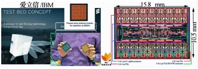

Figure 3 77 GHz radar based on wafer level RF microsystem package of A-star Institute
1.2 technical connotation of RF microsystem integration
The three-dimensional heterogeneous integration technology applied to RF Microsystems is a special manufacturing technology for RF microsystems based on advanced micro nano manufacturing and micro connection packaging technology and integrated with various advanced technologies such as microelectronics, micromachining, micro optics, micro energy and micro flow. It can realize the manufacturing of advanced RF system architecture and greatly improve the performance, Solve the integration bottleneck. In the field of RF applications, such as radar array integration for detection and sensing, micromachining technology mainly solves the application requirements of RF micro system miniaturization, multi-functional integration and high reliability. Its key technologies include TSV / TGV packaging substrate manufacturing technology, multi-functional low loss three-dimensional heterogeneous integration technology, broadband high-power three-dimensional heterogeneous integration technology, etc. At the same time, the micromachining process shall also have the ability of process test, system test and reliability verification. On the one hand, process defects are found in time and optimized to improve the yield of micro machining; On the other hand, the performance of RF micro system is tested to verify and ensure the reliability of the system.
1.3 RF microsystem integration technology system
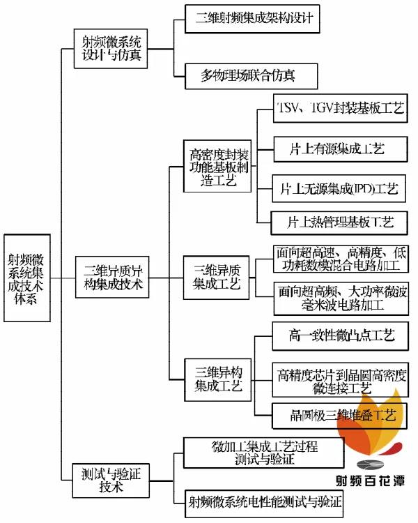
Figure 4 RF microsystem integration technology system
1) RF microsystem design and Simulation Technology
RF microsystem design and simulation include three-dimensional integrated architecture design and multi physical field joint simulation.
Three dimensional integrated architecture design includes circuit module distribution design, three-dimensional RF transmission architecture design and crosstalk shielding design technology. Realize the signal integrity and power integrity evaluation of active and passive circuit networks in three-dimensional integrated packaging to avoid electromagnetic interference. Finally, the functional design contents of transceiver channel, power management, control and power division network in RF micro system can be completed. Multi physical field joint simulation includes thermal mechanical electrical collaborative simulation, reliability evaluation simulation design and so on. Due to the coupling of electromagnetic, thermal, stress and other physical fields in three-dimensional packaging after the miniaturization of RF system, a mixed multi physical characteristic compatibility problem has been formed. RF micro system will encounter problems such as heat dissipation, structural reliability, power on condition reliability and so on. Therefore, it is necessary to use multi physical field joint simulation to realize the thermal effect distribution and heat dissipation channel design in RF micro system, and realize the comprehensive design of mechanical, electrical, thermal and electromagnetic compatibility of RF micro system.
2) 3D heterogeneous integration technology
(1) the high-density packaging substrate constitutes the basic framework of RF microsystem integration. In the RF microsystem architecture, the functions of electrical interconnection, functional integration and structural support between RF modules and RF subsystems are realized. TSV / TGV packaging substrate process capability, on-chip active integration process capability, on-chip passive integration process capability and on-chip thermal management substrate process capability are required. In order to meet the needs of complex electrical interconnection, low loss transmission and high integration of RF micro systems, relevant micromachining process capabilities need to include silicon / glass based high aspect ratio etching, active chip embedding, multilayer rewiring, on-chip resistance capacitance sensing (RCL) integration and other process and technical capabilities.
(2) three dimensional heterogeneous integration provides a solution for the integration of multi-functional chip devices in RF microsystems. It meets the micromachining requirements of multi-functional radio and digital processing chips in RF microsystems through the processing capabilities of ultra-high speed, high-precision and low-power digital analog hybrid circuits and ultra-high frequency, high-power microwave and millimeter wave circuits, It includes core technologies such as high-speed, high-precision and wide-band digital to analog / analog-to-digital conversion (DAC / ADC) heterogeneous integration, compound semiconductor and silicon-based monolithic heterogeneous integration.
(3) the three-dimensional heterogeneous integration process has the natural advantage of combining RF micro module, photoelectric transmission micro module and signal processing micro module in heterogeneous form to meet the integration requirements of multi-functional RF micro system. Three dimensional heterogeneous integration process requires several capabilities, such as high consistency micro bump process, high-precision chip to wafer high-density micro connection process and wafer level three-dimensional stacking process. In order to meet the requirements of three-dimensional, high-precision and small pitch micromachining of RF micro system, key technical capabilities such as alloy and metal bump preparation technology, high-precision flip chip welding technology and wafer bonding technology are required.
3) RF microsystem integration process test and verification technology
RF micro system needs to carry out process quality monitoring, failure analysis, circuit nondestructive testing and fault troubleshooting and diagnosis of each step, and needs to have the ability of micro machining process testing and verification, which can be divided into two parts: micro machining integrated process testing and verification and RF micro system electrical performance testing and verification. According to the electrical performance and material stress test requirements of RF micro system TSV / TGV substrate, functional layer wafer and other components, it can be further subdivided into key technologies such as TSV / TGV packaging substrate electrical performance test technology, micromachining process stress and thermal failure detection and analysis technology.
2 RF microsystem integration technology
2.1 advantages of RF microsystem integration technology bring opportunities for industrial development
The advantages of RF microsystem technology can be summarized as "smaller, more, stronger and newer". What's more, the scale of system integration has developed from extensive macro size to fine micro nano size, which shows that the volume, weight and power consumption are significantly reduced; More refers to the development of system function from single function to multi-function, and the function density is increased by 1 ~ 2 orders of magnitude; Stronger means that the system performance is stronger. In addition to the significant improvement of bandwidth and speed, it is also developing to the intelligent level of reconfiguration, adaptation and autonomy; Update refers to the adoption of new integration means to make new concepts, new systems and new modes centrally reflected in the microsystem.
RF micro system technology can promote the development of military and civilian electronic information systems to chip and skin, meet the requirements of the next generation advanced integration of military weapon platform loads and civil products, promote the chip and generalization of RF systems, and reduce the development cost and cycle; In terms of function, promote the digitization, multi-function integration and intelligence of the whole machine, and give birth to the reform of weapon system and civil electronic product system. Actively integrate civil advanced semiconductor integration technology and standardized packaging integration technology, reduce the complexity of military equipment and civil electronic facilities, shorten the development cycle and improve maintainability, so as to make the vision of large-scale production, cost reduction and efficiency increase of the next generation RF system possible. The establishment and improvement of the micro system industry will promote the integration of the original industrial chain and bring about significant changes in the form and connotation of the existing electronic information products.
The micro system RF module integrates and packages the power supply, wave control, RF and other chips through a high-density adapter substrate to realize the multi-function, miniaturization and high reliability of the module. Due to the improvement of integration density and working frequency, the architecture design of Microsystem products brings many technical challenges to the structure, process and circuit design: firstly, the problems of signal isolation and mutual interference, power supply and signal integrity, cavity effect and so on put forward higher requirements for system layout and wiring; Secondly, the increase of chip heat consumption and size and the decrease of interconnection spacing highlight the problem of thermal stress failure caused by material thermal matching; Finally, the reduction of interconnection spacing and the increase of port number, high-precision three-dimensional lamination, multi temperature gradient welding and product repairability put forward more stringent requirements for process and materials. Therefore, with the continuous compression of product development cycle, the realization and engineering application of Microsystem modules need multi-disciplinary and multi field collaborative design such as structure, telecommunications, process and thermal design.
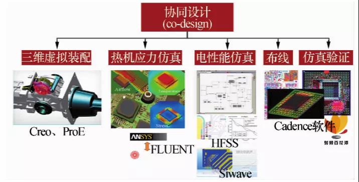
At present, the development of typical microsystem products first needs to carry out architecture design, complete the preliminary layout of products, determine the preliminary process route, and complete the selection of materials and key devices; On this basis, according to the characteristics of materials and key components, carry out three-dimensional virtual assembly, thermal engine stress simulation analysis, electromagnetic shielding isolation, cavity effect, signal and power integrity, RF field circuit simulation analysis, and optimize the structural layout according to the simulation results; Then, the wiring design and simulation verification of the substrate are carried out; Finally, carry out physical verification and optimize and finalize the design scheme (as shown in Figure 5).
With the improvement of micro system integration, the volume and power consumption are significantly reduced, but the problem of thermal effect is becoming more and more prominent, which may lead to the deterioration of device performance and even failure. The heat flux density of power components widely used in military electronic systems is higher, the application environment is also worse, and its thermal management is more difficult. Without good cooling measures, the chip temperature will reach 6000 ℃ in the future. Therefore, the performance of micro system is ultimately restricted by the heat dissipation capacity, and its thermal management technology is an urgent technical problem to be solved. For 3D packaged Microsystems, new heat dissipation technologies have been gradually developed. Five new heat management technologies under development and their characteristics are shown in Table 1.
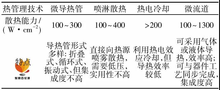
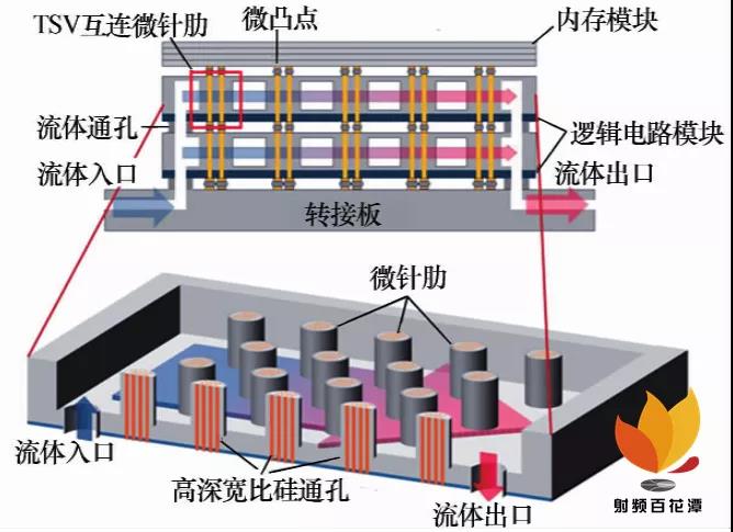
Silicon based microchannel integration technology is a hot spot in the research of efficient heat dissipation, in which the micro pin rib structure integrating TSV is one of the typical technologies of efficient thermal management of microsystem. This technology makes a large number of micro pin ribs in the silicon adapter plate, and the heat is transmitted to the coolant through the upper and lower surfaces of the cavity around the micro pin rib. Compared with the traditional micro channel, it greatly improves the heat dissipation capacity. At the same time, the TSV array made inside the microneedle rib not only realizes the fluid transmission, but also ensures the high-density transmission of electrical signals (as shown in Fig. 6). However, most cooling systems based on chip or board microchannels need to have an interface with the outside world. The volume and size of this interface may far exceed the size of the chip. These problems still need to be studied and solved in the future.
During the development and production of RF microsystem products, layered testing and three-dimensional post stack testing are required. Figure 7 shows the typical three-dimensional system level packaging (SIP) module test mode with RF microsystem characteristics. RF micro system products have high working frequency, small interconnection spacing and many input / export ports. In order to ensure the subsequent normal assembly and use, they have extremely high requirements for nondestructive testing. Therefore, it brings great challenges to the design of test fixture, which is embodied in the following four aspects:


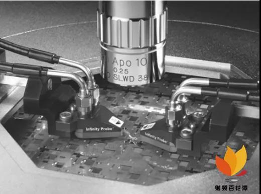
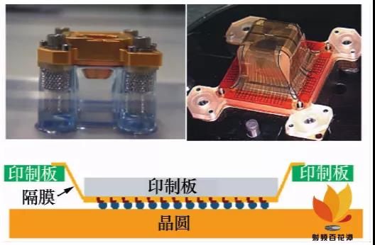
The RF micro system with all silicon-based three-dimensional heterogeneous integration features smaller pad spacing (tens of microns), higher integration, and the machining accuracy of the test fixture is difficult to meet the requirements. The technology and concept of wafer test of the probe table are needed. Due to the existence of RF input / output ports on both sides of micro system three-dimensional heterogeneous integration products, the existing mature wafer test methods still can not meet the requirements, especially in the millimeter wave band, there is no mature solution at home and abroad. At present, wafer single-sided test screening is mainly conducted on the probe table with the help of probes and custom probe cards, as shown in Figure 9; For the wafer level screening test of micro bumps such as Cu pillar, foreign manufacturers such as cascade have also launched pyramid membrane microwave probe card, as shown in Figure 10.
In the whole life cycle of Microsystem products, there are many problems and challenges, among which the process problems in the processing process and the reliability problems in the application process must be considered. At present, the main process problems include the yield of TSV in three-dimensional integrated microsystem, wafer thinning and transmission, multilayer chip stacking, low radian wire bonding, etc. the reliability problems include process reliability, thermal mismatch reliability, anti-interference reliability, etc.
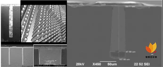
There are many processes involved in TSV vertical interconnection, including deep hole etching process, side wall insulation process, preparation of adhesive layer and seed layer, TSV deep hole filling process, etc. Whether each process is good or not will directly affect the yield of TSV. There are a large number of TSVs applied in high-density microsystem integration. How to ensure the yield of TSV is an important process problem. Figure 11 shows the high-density TSV structure and TSV defect problems caused by poor TSV filling.
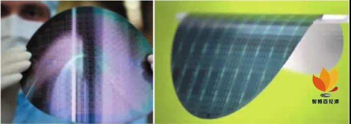
Thinning process is a necessary process for the development of micro system to miniaturization, which can reduce the volume of the system in the Z direction. As the wafer becomes further ultra-thin (thickness reaches 50) μ m) , it will present flexible characteristics, which will bring great difficulties to the further thinning of the wafer and the transmission of the back channel. Figure 12 shows the flexible characteristics of the wafer after thinning to a certain thickness. Stacking process is one of the cores of the whole three-dimensional heterogeneous integration process of microsystem, and it is also an indispensable process to realize high-density integration of microsystem. Through the stacking process, not only the physical fixation of the micro system, but also the excellent electrical interconnection needs to be realized. Ensuring the quality of stacking process is the top priority to realize microsystem integration.
Some micro nano manufacturing processes make it necessary to consider the reliability of the micro system in the machining process. Especially with the improvement of the integration and complexity of the micro system, the process manufacturing process has become more complex. All process flows have brought great challenges to the process reliability. Figure 13 shows the solder joint cracking caused by the interaction between processes. At the same time, with the increasing heat consumption of SOC chip and sip system, the increase of package size and the difference of thermal expansion coefficient between different materials, it brings challenges to the reliability design of the system. Figure 14 shows the thermal mismatch problem in the package.

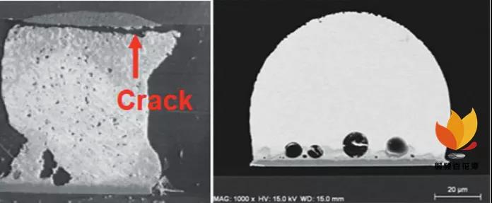
Figure 14 example of thermal mismatch problem
3 development ideas of RF microsystem integration technology
(1) integrate the advantageous resources of the micro system industrial chain, organically combine industry, University, research and application represented by domestic universities and industrial sector research institutions, establish an open and engineering micro system technology platform, and establish a collaborative R & D team integrating design, simulation, process and testing, so as to form a collaborative innovation development pattern of micro system.
(2) strengthen the construction of Microsystem capacity, promote the distribution construction of existing microsystem capacity to centralized construction, form the rapid iteration ability of R & D and trial production, and accelerate the engineering transformation progress of Microsystem integration technology.
(3) give priority to the development of Microsystem technologies that meet the urgent needs of the country and can make key breakthroughs in a short time; Focus on promoting the research of some key microsystem technologies with important industrialization prospects and promoting the development of the national economy, encourage the key basic research of microsystem, and promote original innovation.
(4) focus on the successful development of representative products, gradually radiate to the fields of RF micro system and photoelectric micro system with higher technical capacity and stronger performance, focus on the common technologies in various fields, break through the bottleneck technologies one by one, and form a diversified trial production and R & D capacity of micro electronic information system.
(5) pay attention to the cultivation of core and key talents, build a high-quality microsystem research, development and application team, and ensure the sustainable development of microsystem technology.
4 Conclusion
Microsystem technology is the inevitable result of people's continuous pursuit of miniaturization and high performance of electronic information equipment since the advent of microelectronics technology. It is a model of the integrated development of application innovation and technological innovation. This paper expounds the application requirements and development trend of RF microsystem integration technology in military and civil fields, combs the system framework of RF microsystem integration technology, studies and judges the challenges and development opportunities faced by the technology, and puts forward the further development ideas of RF microsystem integration technology. The innovation and development of microsystem technology will not only promote the subversive progress of weapons and equipment in the future, but also accelerate the great leap forward development of civil information industry.
The "kinghelm" trademark was originally registered by golden beacon company. Golden beacon is a direct selling manufacturer of GPS antenna and Beidou antenna. It has a very high popularity and reputation in Beidou GPS navigation and positioning industry. The R & D and production products are widely used in BDS satellite navigation and positioning, wireless communication and other fields. The main products include: rj45-rj45 network, network interface connector, RF connector adapter, coaxial cable connectorType-C connectorHDMI interface, type-C interface, pin and bus arrangementSMA, FPC, FFC antenna connector, antenna signal transmission waterproof connector, HDMI interface, USB connector, terminal line, terminal board terminal block, wiring terminal block, RF RFID tag, positioning and navigation antenna, communication antenna antenna connecting line, rubber stick antenna sucker antenna, 433 antenna line, 4G antenna, GPS module antenna, RG113, RG178, rg316, FPC flexible cable is matched with FPC connector, Network cable interface, etc. It is widely used in aerospace, communication, military industry, instrumentation, security, medical and other industries.
The content comes from the network/High speed RF Baihuatan, this website only provides reprint. The views, positions and technologies of this article have nothing to do with this website. If there is infringement, please contact us to delete it!
Copyright © Shenzhen Kinghelm Electronics Co., Ltd. all rights reservedYue ICP Bei No. 17113853