Service hotline
+86 0755-83975897
Release date:2021-12-28Author source:KinghelmViews:2653
一、Basic concepts of impedance measurement
Impedance definition:
Impedance is the total reaction of components or circuits to periodic AC signals.
AC AC test signal (amplitude and frequency).
Including real part and imaginary part.
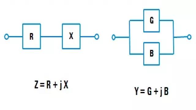
Figure 1 definition of impedance
Impedance is an important parameter for evaluating circuits, components and manufacturing component materials. So what is impedance? Let's first look at the definition of impedance.
First, the impedance is a vector.
Generally, impedance refers to the resistance of a device or circuit to AC current flowing through it at a given frequency. It is represented by the complex number on the vector plane. An impedance vector includes a real part (resistance R) and an imaginary part (reactance x). As shown in Figure 11-1, impedance is represented by z = R + JX in rectangular coordinate system. Then in the polar coordinate system, the impedance can be expressed by amplitude and phase angle. The real part and imaginary part in rectangular coordinate system can be mathematically converted into amplitude and phase in polar coordinate system.
Second, remember that the unit of impedance is Ohm. In addition, consider that the well-known resistance (R), inductance (L) and capacitance (c) correspond to the position in the complex impedance plane respectively.
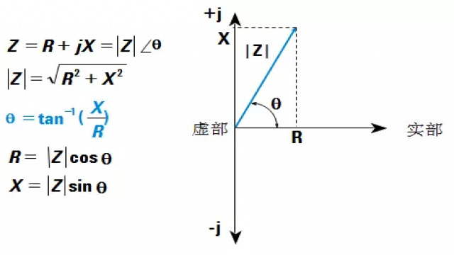
Figure 2 formula of impedance
What is admittance?
Admittance is the reciprocal of impedance. It can also be expressed as real part (g conductivity) and imaginary part (susceptance). Its unit is Siemens.

Fig. 3 formula of admittance
Why are there two expressions of impedance and admittance? It is mainly to express two common serial and parallel connection modes very simply. When resistance and reactance are connected in series, the expression of impedance is very simple and easy to use. However, when the resistance and reactance are connected in parallel, the expression of impedance is very complex. At this time, the use of admittance is very simple and easy to use.
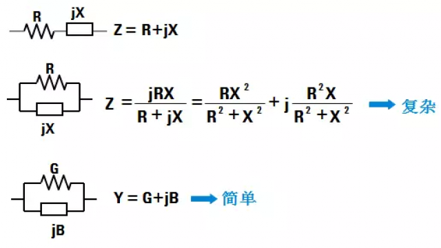
Fig. 4 Relationship between impedance and admittance
Relationship between impedance and inductance L and capacitance C:
There are two forms of reactance - inductive reactance (XL) and capacitive reactance (XC). Inductance corresponds to inductive reactance and capacitance corresponds to capacitive reactance. For ideal inductance and capacitance, they are proportional and inversely proportional to inductive reactance and capacitive reactance respectively. By definition,
XL=2pfL=wL
XC= 1/2pfC=1/wC
F is the frequency of the AC signal, l is the inductance and C is the capacitance. The unit of inductance is Heng and the unit of capacitance is fa.
W is the angular velocity, w = 2pF.
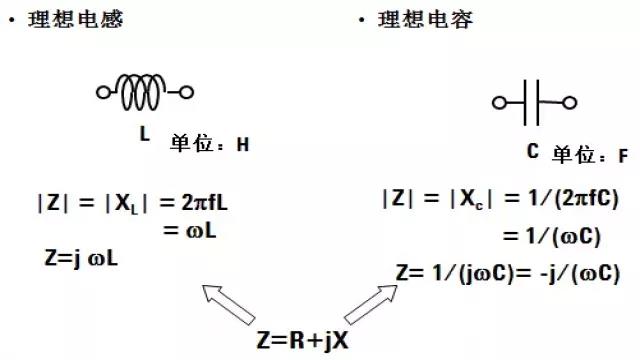
Fig. 5 Relationship between impedance and capacitance / inductance
If the impedance vs frequency diagram of the inductance is also drawn in the same impedance diagram, it is not difficult to find that the impedance of the inductance increases with the increase of frequency, and the impedance of the capacitance decreases with the increase of frequency. Even for ideal inductors or capacitors, their impedance changes with the frequency of the incident AC signal.
Quality factor Q and loss factor D:
Quality factor Q is an index to measure the purity of reactance (and susceptance). In other words, the quality factor Q indicates that the device is close to the pure reactance. The greater the quality factor, the greater the absolute value of the reactance. Conversely, the smaller the resistance of the device.
In fact, the real part of the device impedance, that is, the resistance, indicates the loss of energy after energy is transmitted through the device. Therefore, it can be seen from the above formula that the quality factor indicates the degree of energy loss of the device.
The quality factor (q) is a measure of the purity of reactance (i.e. the proximity to pure reactance, i.e. no resistance), which is defined as the ratio of the energy stored in the element to the energy lost by the element.
Q is a dimensionless unit, and the expression is q = x / r = B / g. You can see from Figure 6 that Q is the tangent of the Q angle.
Q is generally applicable to inductors. For capacitors, the term indicating purity is usually represented by dissipation factor (d). The dissipation factor is the reciprocal of Q, which is also the tangent of the Q complement angle, and the D angle is shown in Fig. 6.
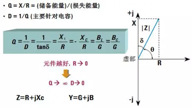
Figure 6 quality factor and loss factor
Actual capacitance model:
Let's take a closer look at real capacitive devices. First of all, we should be clear that different materials and manufacturing technologies will cause different sizes of parasitic parameters. The leads of the device will produce unwanted series resistance and inductance, and there will be parasitic parallel resistance and parasitic capacitance at both ends of the device. So as to affect the usability of the element and the accuracy of the determined resistance, capacitance or inductance.
A real-world component contains many parasitic parameters. As a combination of main parameters and parasitic parameters of components, as shown in the figure above, a component is like a complex circuit.
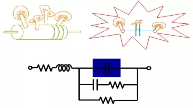
Figure 7 actual capacitance model
Why test impedance?
The impedance of the element is affected by many factors
Frequency
Test signal
DC offset
Temperature
Other
Due to parasitic parameters, the frequency has an impact on all actual components. Not all parasitic parameters will affect the measurement results, but it is some main parasitic parameters that determine the frequency characteristics of the element. When the impedance values of the main components are different, the main parasitic parameters will also be different. Figs. 8 to 10 show typical frequency responses of actual resistors, inductors, and capacitors.
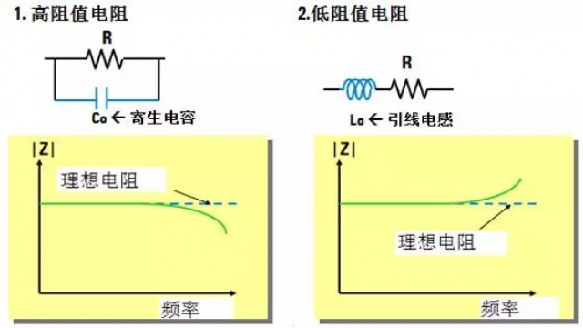
Fig. 8 Effect of frequency on resistance impedance
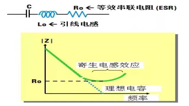
Fig. 9 Effect of frequency on inductance impedance
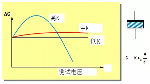
Fig. 10 effect of frequency on capacitance impedance
Influence of AC signal level (capacitance):
The SMD capacitance (with different dielectric constant, K) related to AC voltage is affected by AC test voltage, as shown in Figure 11.
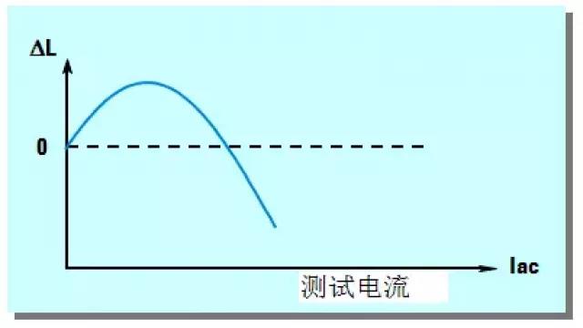
Fig. 11 capacitance affected by AC test voltage
The magnetic core inductor is affected by the electromagnetic hysteresis characteristics of the coil material, and the inductance of the coil inductance will change with the change of the test signal current, as shown in FIG. 12.
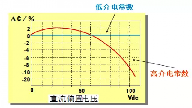
Fig. 12 magnetic core inductor affected by AC test current
DC bias will also change the characteristics of the device. It is well known that DC bias affects the characteristics of semiconductor devices, such as diodes and transistors and other passive devices / passive devices. For capacitors made of high dielectric constant materials, the higher the DC bias voltage applied to the device, the greater the change of capacitance.
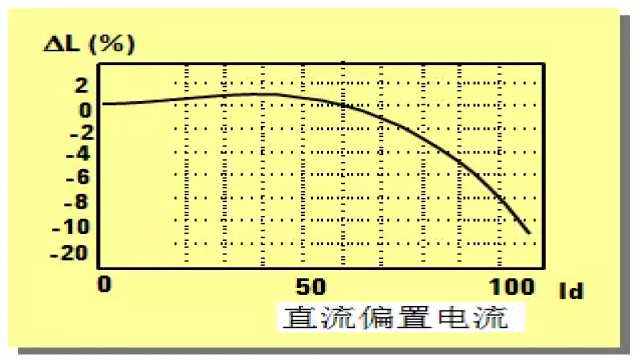
Figure 13 ceramic capacitor affected by DC bias level
For core inductors, the inductance varies with the DC flowing through the coil, which is mainly due to the magnetic flux saturation characteristics of the coil material.
Now, switching power supply is very common. Power inductors are usually used to filter RF interference and noise due to high current switches. In order to maintain good filtering characteristics and reduce the ripple of large current, the characteristics of power inductor must be measured under working conditions to ensure that the rolling characteristics of inductor do not affect its working characteristics.
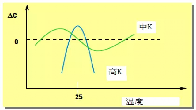
Fig. 14 core inductor affected by DC bias current
Most devices are susceptible to temperature. For resistance, inductance and capacitance, temperature characteristic is a very important specification parameter. The curve below shows the correlation between ceramic capacitance with different dielectric constant and temperature.

FIG. 15 ceramic capacitance affected by temperature
二、Impedance measurement method and principle
There are many alternative methods for impedance measurement, and each method has its own advantages and disadvantages. It is necessary to first consider the requirements and conditions of measurement, and then select the most appropriate method. Factors to be considered include frequency coverage, measurement range, measurement accuracy and convenience of operation. No one method can include all the measurement capabilities, so a compromise is needed in the selection of measurement methods. The following focuses on three methods according to the characteristics of high-speed digital circuits. If only the measurement accuracy and operation convenience are considered, the automatic balance bridge is the best choice until the frequency of 110Mhz. For the measurement from 100MHz to 3GHz, the RF I-V method has the best measurement ability, and the network analysis technology is recommended for others. 2.1 automatic balance bridge method
The current flowing through the DUT also flows through resistor RR. The potential at the "L" point is maintained at 0V (thus called "virtual ground"). The I-V conversion amplifier balances the current on the RR with the current of the DUT. The impedance value of the DUT can be calculated by measuring the high-end voltage and the voltage on RR.
The actual configuration of automatic balance bridge of various instruments will be different. The low frequency range of conventional LCR meter is generally lower than 100kHz, and a simple operational amplifier can be used as its I-V converter. Due to the limitation of amplifier performance, this kind of instrument has poor accuracy at high frequency. The I-V converter used in broadband LCR meter and impedance analyzer includes complex detector, integrator and vector modulator to ensure high accuracy in a wide frequency range above 1MHz. This kind of instrument can reach the highest frequency of 110Mhz.
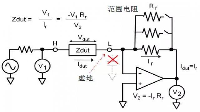
Figure 16 principle of automatic balance bridge method
Advantages and disadvantages of automatic balance bridge method:
The most accurate, basic test accuracy 0.05%
Widest impedance measurement range: C, l, D, Q, R, x, G, B, Z, y, O
Widest range of electrical test conditions
Easy to use
Low frequency, f < 110MHz
2.2 RF I-V method
RF I-V method uses impedance matching measuring circuit (50 ohm) and precision coaxial test port to realize different configurations, and can work at higher frequency. There are two ways to place a voltmeter and an ammeter to accommodate low impedance and high impedance measurements, respectively. As shown in the figure, the impedance of the device under test (DUT) is derived from the measured values of voltage and current, and the current flowing through the DUT is calculated from the voltage on the low resistance resistor R with known resistance. In actual measurement, a low loss transformer is placed at resistor R, but the transformer also limits the low end of the applicable frequency range.
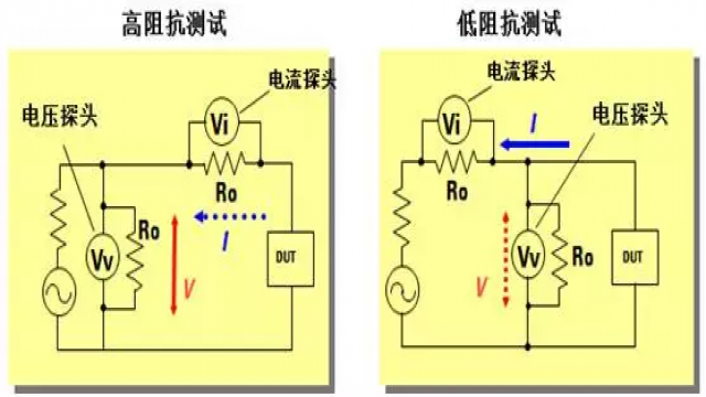
Figure 17 RF I-V method
Advantages and disadvantages of RF I-V method
Wide / high frequency range, 1MHz < f < 3GHz
Good test accuracy, basic test accuracy 0.8%
Wide impedance measurement range, 100m – 50KW @ 10% accuracy
100MHz the most accurate test method
Grounding device test
2.3 Network segmentation
The reflection coefficient is obtained by measuring the ratio of the injected signal to the reflected signal. The reflected signal is detected by directional coupler or bridge, and the signal is provided and measured by network analyzer. Since this method measures the reflection on the DUT, it can be used in a higher frequency range.
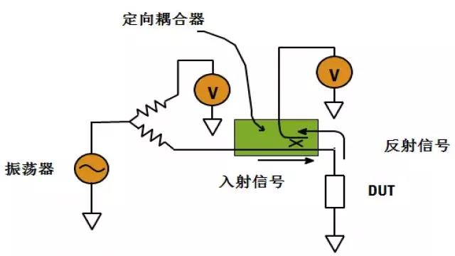
Figure 18. Network analysis method
According to the actual measurement requirements, the network analysis method extends several methods to improve the impedance range of the test.
2.3.1 Reflection method
This is the most typical network analysis method. Test the impedance by testing S11. The formula is as follows:
ZDUT=50(1+S11)/(1-S11)
For e5061b network analyzer:
Frequency range measurable: 5Hz to 3GHz
10% accuracy impedance range: 1 ohm ~ 2K ohm
7mm type series test fixture can be used
2.3.2 Series straight through method
As shown in the figure, the series through method connects the measurement DUT in series. For e5061b, both gain phase test port and S-parameter test port can use the series through method. In contrast, the gain phase test port is more convenient because the 4-terminal device test fixture can be directly connected to the gain phase test port. However, the maximum frequency range is only 30MHz. If you want to test a higher frequency, you can use the S parameter to test the port. However, when the frequency reaches several hundred megabytes, it is difficult to eliminate the error caused by the series through test fixture. Therefore, the actual frequency limit is about 200MHz or 300MHz.
For e5061b network analyzer:
Frequency range measurable: 5Hz to 30MHz (gain phase test port)
5Hz to hundreds of MHz (s parameter test port)
10% accuracy impedance measurement range: 5 ohms to 20K ohms
Available test fixture (gain phase test port)
Not applicable to measurements connected to the DUT
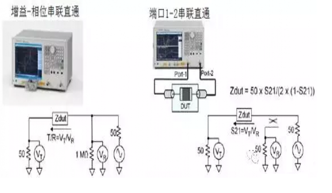
Figure 19 series straight through method
2.3.3 Parallel straight through method
As shown in the figure, the parallel through method tests the impedance through parallel DUTs. This method is very suitable for measuring low impedance devices, which can be as small as 1m ohm. Both gain phase test port and S-parameter test port can use parallel straight through method. For the frequency range exceeding 30MHz, use the S-parameter test port for parallel through test. However, for less than 100kHz, it is recommended to use the gain phase test port for impedance measurement, because the efficiency phase test port uses the semi floating design method, which can eliminate the resistance error caused by the return current in the test cable shielding layer, so that the very low impedance can be easily and accurately measured in the low frequency range.
For e5061b network analyzer:
Frequency range: 5Hz to 30MHz (gain phase test port), 5Hz to 3GHz (s parameter test port 1-2)
10% accuracy impedance measurement range: 1m ohm to 5 ohm (higher measurement sensitivity than impedance analyzer). Use self-made test fixture or RF probe

Figure 20 parallel straight through method
2.4 Typical impedance measuring instrument
The three most typical impedance measuring instruments in the industry are 4294A, e4991a and e5061b. Their characteristics are as follows:
4294A precision impedance analyzer:
The measurement frequency ranges from 40 Hz to 110 MHz
The basic measurement accuracy is & plusmn; 0.08%
The industry's highest performance impedance measurement and analyzer
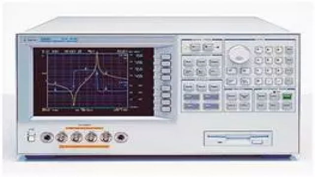
Figure 21 4294A precision impedance analyzer
E4991a RF impedance / material measurement analyzer:
The measurement frequency range is from 1 MHz to 3GHz
The basic measurement accuracy is & plusmn; 0.8%
The material measurement function can measure dielectric constant and permeability (configuration option 002)
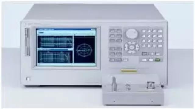
Figure 22 e4991a RF impedance / material measurement analyzer
E5061b vector network analyzer
Measurement frequency range on S parameter measurement port: from 5 Hz to 3 GHz
Measurement frequency range on gain phase measurement port: from 5 Hz to 30 MHz
The basic measurement accuracy is & plusmn; 2%
PDN (Power Distribution Network ——Milliohm impedance value test of power supply distribution network (bypass capacitor, output impedance of switching power supply (DC-DC converter), impedance of PCB board, etc.)
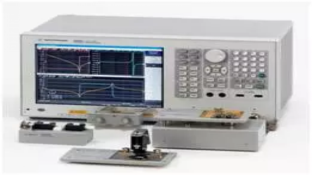
Figure 23 e5061b vector network analyzer
Comparison of impedance measurement ranges of various instruments when the measurement accuracy is 10%.
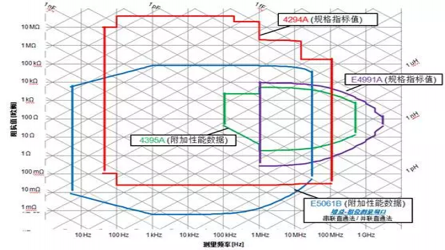
Fig. 24 comparison of impedance measurement ranges of three typical instruments
三、Test error and calibration and compensation
3.1 Measurement error
For real-world measurements, we must consider that errors are included in the measurement results. Common error sources are: instrument inaccuracy (including DC bias inaccuracy and OSC level inaccuracy), residual parameter noise in test fixture and cable
The parasitic parameters of the DUT are not listed here because the parasitic parameters of the DUT are part of the DUT. We need to measure the DUT impedance including its parasitic parameters. Among the listed error sources, if the residual impedance of the test fixture and test cable is constant and stable, it can be compensated.
3.2 Calibration
Calibration is defined by "calibration plane", on which the specified measurement accuracy can be obtained. To calibrate the instrument, connect the "standard device" on the calibration plane, and then adjust the instrument (through calculation / data storage) to make the measurement results within the specified accuracy range.
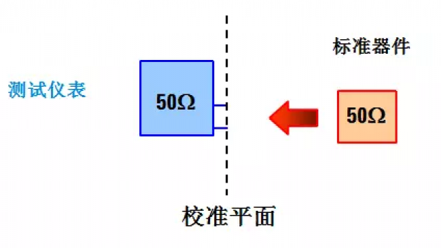
Figure 25 calibration and its calibration plane
The calibration plane of the automatic balance bridge instrument is an unknown BNC connector. After performing the cable length calibration, move the calibration plane to the top of the test cable. The calibration of automatic balance bridge instrument is usually for operation and maintenance. In order to maintain the instrument within the specified accuracy, it should be calibrated periodically (typically once a year).
RF I-V instruments require calibration every time they are turned on or the frequency setting is changed. Because at high frequency, the surrounding temperature, humidity and frequency setting have a great impact on the measurement accuracy. Open circuit, short circuit and standard load (low loss capacitance is sometimes required) are required for calibration. The calibration plane is at the position of the connector connecting the calibration piece.
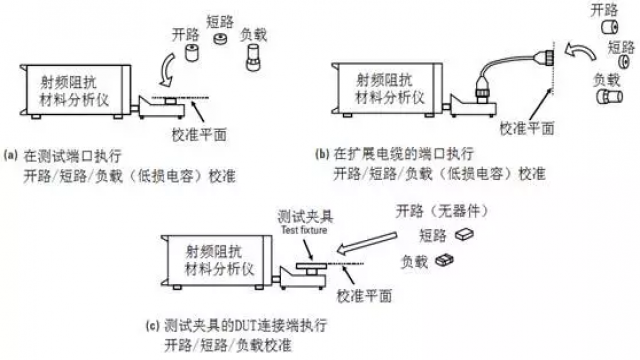
Figure 26 calibration method and calibration plane of RF I-V instrument
3.3Compensate
Compensation can reduce the influence of error source between DUT and instrument calibration plane. However, the compensation can not completely eliminate the error, and the measurement accuracy obtained after compensation can not reach the accuracy obtained on the "calibration plane". Compensation is different from calibration, and it cannot replace calibration, so compensation must be carried out after calibration. Compensation can effectively improve the measurement accuracy of the instrument. Here are three common compensation technologies.
3.3.1 Offset compensation
When the measurement is only affected by a single residual component, the effective value can be obtained by subtracting the error value from the measured value. In the case of low value capacitance measurement as shown in the figure below, the stray capacitance CO in parallel with DUT capacitance CX has the greatest impact on the measurement results, which can be compensated by subtracting the stray capacitance from the measured value cm. The stray capacitance value can be obtained when the measuring terminal is open circuit.
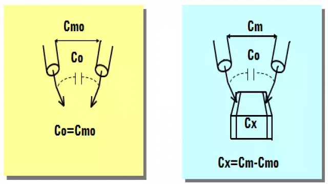
Figure 27 offset compensation
3.3.2 Open and short circuit compensation
Open circuit and short circuit compensation is the most commonly used compensation technology in impedance measurement instruments. This method assumes that the residual parameters of the test fixture can be represented by a simple L / R / C / g circuit, as shown in figure (a) below. When the unknown terminal is open, as shown in figure (b) below, take the measured stray admittance go + jwco as yo, because the residual impedance ZS can be ignored. When the unknown terminal is short circuited, as shown in figure (c) below, the measured impedance represents the residual impedance ZS = RS + jwls, because yo is bypassed. In this way, since each residual parameter is known, the impedance zdut of the DUT can be calculated from the formula given in figure (d) below.
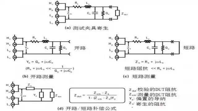
Figure 28 open circuit / short circuit compensation
3.3.4 Open circuit, short circuit and load compensation
There are many measurement conditions, and complex residual parameters cannot be modeled according to the simple equivalent circuit shown in the above figure. Open circuit / short circuit / load compensation is an advanced compensation technology suitable for complex residual circuits. In order to compensate for open circuit / short circuit / load, three measurements must be made before measuring the DUT, that is, open circuit and short circuit at the end of the test fixture, and connect the reference DUT (load). During DUT measurement, the measurement results (data) obtained can be used in the calculation. As shown in the figure below, the residual impedance model of the test fixture established by open circuit / short circuit / load compensation is a 4-terminal network circuit represented by ABCD parameters. If these three items are known and the 4-terminal network circuit is a linear circuit, each parameter can be known.
Open circuit / short circuit / load compensation shall be used in the following cases:
Additional passive circuits or components are connected (such as external DC bias circuits, balanced unbalanced transformers, attenuators and filters).
Use a scanner, multiplexer or matrix switch.
Use non-standard length of test cable or extend 4tp cable by standard Agilent test cable.
Enhance the test signal with an amplifier.
Use the component cartridge.
Use the test fixture made by the user.
Under the conditions listed above, the open / short circuit compensation will not meet the requirements, and the measurement results will have considerable error.
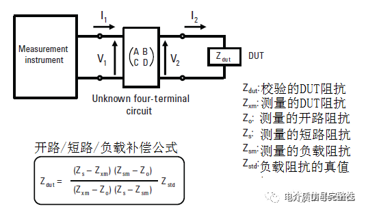
Figure 29 open circuit / short circuit / load compensation
3.4 Error caused by contact resistance
Any contact resistance between DUT electrode and test fixture or test bench electrode will cause test error. The contact resistance of 2-terminal or 4-terminal connection mode of DUT is different. In the case of 2-terminal connection, the contact resistance is superimposed on the DUT impedance in series, resulting in a positive error of D (dissipation factor) reading. In the case of 4-port connection, there are contact resistors RHC, RHP, RLC and RLP as shown in figure (b) below. The influence of contact resistance of different terminals is also different. RHC reduces the test signal level applied to the DUT, but it does not directly produce measurement error. RLP may cause imbalance of automatic balance bridge, but this effect can usually be ignored. RHP and CHP constitute a low-pass filter, which will cause the attenuation and phase shift of HP input signal, resulting in measurement error.
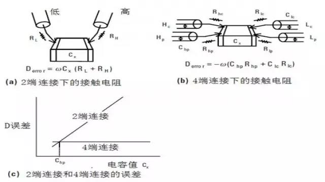
Fig. 30 error caused by contact resistance
3.5 Error introduced by cable expansion
The 4tp measurement cable extended from the instrument will introduce the amplitude error and phase shift of the measurement signal according to the length and measurement frequency of the extended cable. Cable expansion brings the following two problems:
Error in impedance measurement and bridge imbalance
The measurement error is mainly caused by the cables connected to HP and LC ends. If the length and propagation constant of the cable are known, the instrument can compensate it. The phase shift of the feedback loop including RR, amplifier and LP and LC cables will cause the imbalance of the bridge. However, phase shift compensation can be carried out inside the feedback circuit. Only in the higher frequency region (usually higher than 100kHz), these two problems have a significant impact, and Agilent impedance test instrument can compensate for the cable provided by Agilent. In the lower frequency region, the capacitance of the cable will only reduce the measurement accuracy (without affecting the bridge balance).
Cable length compensation is used for test cables with known length and propagation constant, such as 1m (2m or 4m) test cables provided by Agilent. If cables of different lengths and types are used, in addition to measurement errors, bridge imbalance may also be caused.
3.6Calibration and compensation of parallel straight through method
When e5061b is used to test the milliohm impedance of PDN, the parallel through method also needs to consider calibration and compensation. Generally, when testing low frequency, the gain phase test port is used. Generally, only through calibration can obtain sufficient impedance test accuracy. When testing the high frequency, use the S parameter to test the port, which can be calibrated with sol, or sol calibration plus port extension. If the probe table is used, the calibration piece provided by the probe table can be directly calibrated to the probe tip position with sol.

Fig. 31 calibration and compensation of parallel straight through method for low impedance measurement
四、Test cables and clamps
When connecting the DUT to the measuring terminal of the automatic balance bridge instrument, there are several optional connection configurations. In the RF impedance measurement instrument, the connection configuration of two terminal method can only be used.
4.1 Terminal configuration
The front panel of the automatic balance bridge instrument is generally equipped with four bncunknown terminals (HC, HP, LP and LC). There are various configuration methods for connecting DUT and unknown terminal. Since each method has its own advantages and disadvantages, the most appropriate configuration method must be selected according to the impedance of the DUT and the required measurement accuracy.
2-terminal (2t) configuration:
This is the simplest method, but there are many error sources in this method. The lead inductance, lead resistance, and stray capacitance between the two leads will be superimposed on the measurement results. Due to these error sources, the typical impedance measurement range (without compensation) is limited to 100 ohms to 10K ohms.
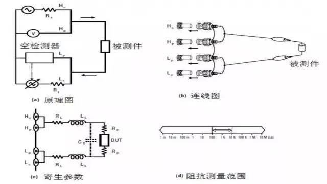
Figure 32 2-terminal (2t) configuration
3-terminal (3T) configuration:
Coaxial cable is used to reduce the influence of stray capacitance. The outer conductor (shield) of the coaxial cable is connected to the protective terminal. It can improve the measurement accuracy in the higher impedance measurement range, but because there are still lead inductance and lead resistance, it can not improve the measurement accuracy in the lower impedance range. The typical impedance range can be extended to more than 10k ohms.

Figure 33 3-terminal (3T) configuration
4-terminal (4T) configuration:
The influence of lead inductance can be reduced because the signal current path and circuit sensitive cable are independent of each other. The accuracy of lower impedance measurement ranges as low as 1 ohm can generally be improved. When the impedance of the DUT is lower than 1 ohm, a large signal current will pass through the current path, and its mutual inductance coupling with the voltage sensitive cable will produce error.
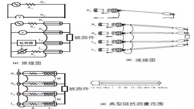
Figure 34 4-terminal (4T) configuration
5-terminal (5T) configuration:
It is a combination of 3T and 4T configurations. It is equipped with four coaxial cables, and the outer conductors of these four cables are connected to the protective end. This configuration has a wide measurement range from 1 ohm to 10m ohm, but the mutual inductance problem still exists.

Figure 35 5-terminal (5T) configuration
Using test cables at high frequencies:
4tp configuration is the best solution for wide range impedance measurement. However, in the basic 4tp measurement, because the cable length must be shorter than the wavelength, the cable length is limited by the measurement frequency. The following formula can be used to determine this limitation: basis of impedance measurement (Continued)
Here: F is the measurement frequency (MHz)
L is the cable length (m)
When the cable length is 1m, the maximum frequency limit is approximately 15MHz. If the cable length or frequency exceeds this limit, the automatic balance bridge may not be balanced. For impedance measurement at higher frequencies (usually above 100kHz), cable length compensation is also required.
4.2 Test fixture
In impedance measurement, the test fixture plays an important role in both mechanical and electrical aspects. The quality of the fixture determines the limit of the total measurement quality.
Agilent provides various types of test fixtures according to the types of tested parts. In order to select the most suitable DUT test fixture, it is required to consider not only the physical layout of the contact, but also the available frequency range, residual parameters, and the allowable DC voltage. The contact end (DUT connection) of the test fixture can be 2 ends or 4 ends to suit different applications.
If the DUT cannot use the test fixture provided by Agilent, a special test fixture for the application can be made. The following key factors need to be considered when making test fixtures.
1.Residual parameters must be minimized.
In order to minimize residual parameters, the 4tp configuration should be as close to the DUT as possible. In addition, the correct protection technology can eliminate the influence of stray capacitance.
2.The contact resistance must be minimized.
Contact resistance will cause nearby errors. In the case of 2tp configuration, it will directly affect the measurement results. The contact electrodes shall be firmly connected to the DUT and kept clean at all times. Electrodes shall be made of corrosion-resistant materials.
3.Contacts must be able to open and short.
Open / short circuit compensation can easily reduce the influence of residual parameters of measuring fixture. For open / short circuit measurement, the contact electrode must be open and short circuited. For open circuit measurements, the contact electrode shall be placed at the same distance as when connected to the DUT. For short circuit measurement, a lossless (low impedance) conductor shall be connected between the electrodes or directly connected to the contact electrode. If you want to keep the electrode in a 4-terminal configuration, you should first connect the current terminal and the potential terminal.
4.3 Test cable
When there is a certain distance between the DUT to be tested and the instrument, it is necessary to expand the test port (unknown terminal) with cable. If the length of the extension cable is not considered, it will not only cause errors, but also lead to the imbalance of the bridge, so that it is impossible to measure.
Agilent has a variety of 1m, 2M and 4m test cables with the instrument. When selecting the test cable, the cable length and the available frequency range must be considered. Because the cable error is known, Agilent instrument can minimize the influence of measuring cable. The test error will increase with the increase of cable length and measurement frequency.
It is recommended not to use cables not recommended by Agilent, and the compensation function of the instrument may not be applicable to non Agilent cables. If non Agilent cables have to be used, the same or equivalent cables as Agilent test cables should be used. For higher frequencies, do not use cables that are not supplied by Agilent. In order to use the expansion cable with 4tp configuration, the cable length shall be 1m or 2m, which can be compensated by measuring instruments. If there is an error in the cable length, it will cause additional error.
4.4 Eliminate the influence of stray capacitance
When the DUT has high impedance (i.e. low capacitance), the influence of stray capacitance can not be ignored. As shown in the figure below, for the example of measuring the DUT with 4-terminal contact, CD is connected in parallel with the DUT. When a conductive plate is placed under the DUT, its combined capacitance (CH / / CL) is also connected in parallel with the DUT, resulting in measurement error. CD can be minimized by placing a protective plate between the high end and the low end. In addition, by connecting the protective end to the conductor, the effects of CH and CL can offset each other.
Fundamentals of impedance measurement (Continued)
Figure 36 protection technology eliminates the influence of stray capacitance
4.5 Terminal configuration and test fixture in RF area
The RF impedance measuring instrument has a precise coaxial test port. In principle, it is a 2-terminal configuration. The central conductor of the coaxial test port connector is the active high-end, and the outer conductor is the grounded low-end. The DUT can only be measured with the simplest 2-terminal connection configuration. The residual inductance, residual resistance, stray capacitance and stray conductance of the test fixture are superimposed on the measurement results (before compensation). Whether RF I-V method or network analysis method, the more the measured impedance deviates from 50 ohms, the lower the RF impedance measurement accuracy. The influence of residual parameters increases with the increase of frequency. The higher the frequency, the narrower the measurable impedance range.
The RF test fixture should be specially designed to make the lead length (electrical path length) between the DUT and the test port as short as possible, so as to minimize the residual parameters. Generally, when the frequency is lower than 100MHz, the error caused by the residual parameters of the test fixture is less than the instrument error, which can be ignored after compensation. However, when measuring the low impedance or high impedance close to the residual parameters, the change of the residual parameters of the test fixture will cause the repeatability of the measurement results. The change of residual parameters and the instability of measurement results depend on the positioning accuracy of DUT on the test fixture terminal. For repetitive measurement, the RF test fixture shall be able to accurately position the DUT on the measurement terminal.
At high frequency (usually higher than 500MHz), the residual parameters of the test fixture have a greater impact on the measurement results, and will narrow the actual measurement range. Therefore, the available frequency range of test fixtures limits the maximum frequency of various test fixtures. The sum of the instrument inaccuracy and the error introduced by the test fixture determines the inaccuracy of the DUT measurement results. Since only 2-terminal configuration can be used, compensation is the key to obtain the best measurement accuracy.
WeChat official account reminds: all kinds of test fixtures have their own characteristics and structure. Since it is not only the residual parameters that affect the DUT measurement value, but also the surrounding environment of the DUT (such as grounding plate, terminal layout, dielectric constant of insulator, etc.), in order to obtain good measurement consistency, the same type of test fixture should be used.
There are two types of RF test fixtures: coaxial test fixture and non coaxial test fixture. The difference lies in their geometric structure and electrical characteristics. The non coaxial test clamp has an open measuring end, which facilitates the connection and disassembly of the DUT. Non coaxial fixture is suitable for testing a large number of devices with high efficiency. However, this high efficiency is at the expense of measurement accuracy at high frequency, because there is discontinuity (mismatch) of electrical characteristics between coaxial connector components and test terminals.
The coaxial test fixture fixes the DUT with a configuration similar to the coaxial end, which is connected to the center electrode and the outer conductor cap electrode of the test fixture. Since a continuous 50 ohm characteristic impedance is maintained from the test port to the DUT, the coaxial test fixture can pass the highest measurement accuracy and the best frequency response. Since a repeatable number of insulator diameters can be selected to minimize the gap between the DUT and the insulator, the DUT can be positioned at the end of the test fixture that can obtain the best repeatability without the skill of the operator. Therefore, the coaxial test fixture can obtain lower additional error and much higher measurement repeatability than the non coaxial test fixture.
Fundamentals of impedance measurement (Continued)
Figure 37 typical RF impedance test fixture
The "kinghelm" trademark was originally registered by golden beacon company. Golden beacon is a direct selling manufacturer of GPS antenna and Beidou antenna. It has a very high popularity and reputation in Beidou GPS navigation and positioning industry. The R & D and production products are widely used in BDS satellite navigation and positioning, wireless communication and other fields. The main products include: rj45-rj45 network, network interface connector, RF connector adapter, coaxial cable connector, type-C connector, HDMI interface, type-C interface, pin and bus, SMA, FPC, FFC antenna connector, antenna signal transmission waterproof connector, HDMI interface, USB connector, terminal line, terminal board terminal, terminal strip, RF RFID tag Positioning navigation antenna, communication antenna connecting wire, rubber rod antenna, sucker antenna, 433 antenna, 4G antenna, GPS module antenna, etc. It is widely used in aerospace, communication, military industry, instrumentation, security, medical and other industries.
This content comes from the Internet / cloud brain think tank. This website only provides reprint. The views, positions and technologies of this article have nothing to do with this website. If there is infringement, please contact us to delete it!
Copyright © Shenzhen Kinghelm Electronics Co., Ltd. all rights reservedYue ICP Bei No. 17113853