Service hotline
+86 0755-83975897
Release date:2021-12-28Author source:KinghelmViews:2738
The circuit board layout of radio frequency (RF) circuit shall be based on understanding the basic principles of circuit board structure, power wiring and grounding. This paper discusses the relevant basic principles, and provides some practical and verified power wiring, power bypass and grounding technologies, which can effectively improve the performance index of RF design. Considering that PLL spurious signal is very sensitive to power coupling, grounding and the position of filter elements in practical design, this paper focuses on the methods of PLL spurious signal suppression. In order to illustrate the problem, this paper takes the PCB layout of max2827 802.11a/g transceiver as a reference design.
When designing RF circuit, the design of power circuit and circuit board layout are often left after the design of high-frequency signal path is completed. For the design without careful consideration, the power supply voltage around the circuit is easy to produce wrong output and noise, which will further affect the performance of RF circuit. Reasonably allocate PCB layersVCC lead with star topology (as shown in Figure 1), and adding appropriate decoupling capacitor to VCC pin will help to improve the performance of the system and obtain the best index.
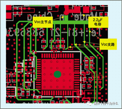
Figure 1: VCC cabling for star topology
Basic principles of power wiring and bypass
Smart PCB layer allocation facilitates the simplification of subsequent wiring processing for a four layer PCB (WLAN
In most applications, the top layer of the circuit board is used to place components and RF leads, the second layer is used as the system ground, the power part is placed in the third layer, and any signal lines can be distributed in the fourth layer. The continuous ground plane layout of the second layer is very necessary to establish an impedance controlled RF signal path. It is also convenient to obtain a ground loop as short as possible, provide a high degree of electrical isolation for the first and third layers, and minimize the coupling between the two layers. Of course, other board layer definitions can also be used (especially when the circuit board has different layers), but the above structure is a proven successful example.
Large area power layer can make VCC wiring easier, but this structure often leads to systemic problems
For a deteriorating fuse, connecting all power leads together on a large plane will not avoid noise transmission between pins. Conversely, if a star topology is used, the coupling between different power pins will be reduced. Figure 1 shows the VCC wiring scheme of star connection, which is taken from the evaluation board of max2826 IEEE 802.11a/g transceiver. In the figure, a main VCC node is established, from which power lines of different branches are led out to supply power to the power pin of RF IC. Each power supply pin uses independent leads to provide spatial isolation between the pins, which is conducive to reducing the coupling between them. In addition, each lead also has a certain parasitic inductance, which is exactly what we want. It helps to filter out the high-frequency noise on the power line.
When using star topology VCC lead, it is also necessary to take appropriate power decoupling, and there is a gap in the decoupling capacitor
Fixed parasitic inductance.
In fact, the capacitance is equivalent to a series RLC circuit. The capacitance plays a leading role in the low frequency band, but at the self-excited oscillation frequency (SRF):

When the frequency is greater than FS, the impedance of the capacitor will show inductance. It can be seen that the capacitor has decoupling effect only when the frequency is close to or lower than its SRF, and the capacitance shows low resistance at these frequency points. Figure 2 shows the typical S11 parameters under different capacitance values. From these curves, we can clearly see the SRF. It can also be seen that the larger the capacitance, the better the decoupling performance provided at lower frequencies (the lower the impedance presented).
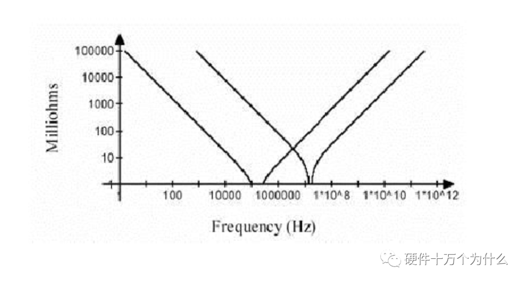
Fig. 2 impedance curves of different capacitances
It is better to place a high-capacity capacitor at the main node of VCC star topology, such as 2.2 & micro; F。 The capacitor has low SRF, which is very effective for eliminating low-frequency noise and establishing stable DC voltage. Each power pin of the IC needs a low-capacity capacitor (such as 10nf) to filter out the high-frequency noise that may be coupled to the power line. For those power pins that supply power to noise sensitive circuits, two bypass capacitors may be required. For example, using a 10PF capacitor in parallel with a 10nf capacitor to provide bypass can provide decoupling in a wider frequency range and eliminate the influence of noise on power supply voltage as far as possible. Each power supply pin needs to be carefully checked to determine how much decoupling capacitance is required and at which frequency points the actual circuit is vulnerable to noise interference.
Good power decoupling technology combined with rigorous PCB layout and VCC lead (star topology) can lay a solid foundation for any RF system design. Although there are other factors that reduce the system performance index in the actual design, having a "noise-free" power supply is the basic element to optimize the system performance.
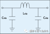
Figure 3: electrical characteristic model of via
Grounding and via design
The layout and leads of the stratum are also the key to the design of WLAN circuit board. They will directly affect the parasitic parameters of the circuit board and have the hidden danger of reducing the system performance. There is no unique grounding scheme in RF circuit design, and satisfactory performance indexes can be achieved in several ways. The ground plane or lead can be divided into analog signal ground and digital signal ground, and circuits with large current or power consumption can also be isolated. According to the previous design experience of WLAN evaluation board, good results can be obtained by using a separate grounding layer in the four layer board. With these empirical methods, the RF part is separated from other circuits by stratum, and the cross interference between signals can be avoided. As described above, the second layer of the circuit board is usually used as the ground plane, and the first layer is used to place components and RF leads.
After the grounding layer is determined, it is very important to connect all signal grounds to the layer with the shortest path. Usually, vias are used to connect the ground wire at the top layer to the layer. It should be noted that vias are inductive. Figure 3 shows the accurate electrical characteristic model of via, in which Lvia is the via inductance and CVIA is the parasitic capacitance of via PCB pad. If the ground wire layout technology discussed here is adopted, the parasitic capacitance can be ignored. A 1.6mm deep via with an aperture of 0.2mm has an inductance of about 0.75nh, and the equivalent reactance in the 2.5ghz/5.0ghz WLAN band is about 12 Ω / 24 Ω. Therefore, a grounding via cannot provide real grounding for RF signals. For high-quality circuit board design, as many grounding vias as possible should be provided in the RF circuit, especially for the exposed grounding pads in general IC packaging. Poor grounding will also produce harmful radiation at the receiving front end or power amplifier, reducing the gain and noise figure index. It should also be noted that poor welding of the ground pad can cause the same problem. In addition, the power consumption of the power amplifier also requires multiple vias connecting the formation.

Figure 4 PLL filter element layout taking max2827 reference design board as an example
Filter out the noise of other stages and suppress the local noise, so as to eliminate the cross interference between stages through the power line, which is the benefit of VCC decoupling. If the decoupling capacitor uses the same grounding via, due to the inductive effect between the via and the ground, the vias at these connection points will carry all RF interference from the two power supplies, which not only loses the function of the decoupling capacitor, but also provides another path for interstage noise coupling in the system.
In the later part of this paper, we will see that the implementation of PLL always faces great challenges in system design. In order to obtain satisfactory spurious characteristics, we must have a good ground wire layout. At present, all PLLs and VCOs are integrated into the chip in IC design. Most PLLs use digital current charge pump output to control VCO through a loop filter. Generally, it is necessary to filter the digital pulse current of the charge pump with a second-order or third-order RC loop filter to obtain the analog control voltage. The two capacitors close to the charge pump output must be directly connected to the ground of the charge pump circuit. In this way, the pulse current path of the ground loop can be isolated to minimize the corresponding stray frequency in lo. The third capacitor (for third-order filters) should be directly connected to the VCO layer to avoid the control voltage floating with the digital current. If these principles are violated, it will lead to considerable stray components. Figure 4 shows an example of PCB wiring. There are many grounding vias on the grounding pad, allowing each VCC decoupling capacitor to have its own independent grounding vias. The circuit in the block is a PLL loop filter, and the first capacitor is directly connected to GND_ CP is connected, and the second capacitor (connected in series with an R) rotates 180 degrees to return to the same GND_ CP, the third capacitor is connected with GND_ VCO connection. This grounding scheme can obtain high system performance.
Suppressing PLL spurious signals through appropriate power supply and grounding to meet the requirements of 802.11a/b/g system transmission spectrum template is a difficulty in the design process. It is necessary to balance the linearity index and power consumption, and leave a certain margin to ensure compliance with IEEE and FCC specifications on the premise of maintaining sufficient transmission power. The typical output power required by IEEE 802.11g system at the antenna end is 15dBm and - 28dbr when the frequency deviation is 20MHz. The power rejection ratio (ACPR) of adjacent channels in the frequency band is a function of the linear characteristics of the device, which is correct for a specific application on a certain premise. A lot of work on optimizing ACPR characteristics in transmission channel is realized by adjusting the bias of TX IC and PA based on experience, and tuning the matching network of input stage, output stage and intermediate stage of PA.
However, not all the problems causing ACPR are attributed to the linear characteristics of the device. A good example is that after a series of adjustments and optimization of the power amplifier and PA driver (the two factors that play a major role in ACPR), the adjacent channel characteristics of WLAN transmitter still can not meet the expected indicators. At this time, it should be noted that the stray signal from the local oscillator (LO) in the transmitter PLL will also degrade the ACPR performance. The spurious signal of Lo will be mixed with the modulated baseband signal, and the mixed components will be amplified along the expected signal channel. This mixing effect will cause problems only when the stray component of PLL is higher than a certain threshold. When it is lower than a certain threshold, ACPR will be mainly restricted by PA nonlinearity. When TX output power and spectrum template characteristics are "linear Limited", we need to balance the linear index and output power; If the lo spurious characteristic becomes the main factor restricting the ACPR performance, we will face the "spurious limitation". We need to bias the PA at a higher operating point under the specified pout to weaken its impact on ACPR, which will consume more current and limit the flexibility of design.
The above discussion raises another problem, that is, how to effectively limit the spurious component of PLL within a certain range so that it does not affect the transmission spectrum. Once the spurious component is found, the first idea is to narrow the bandwidth of the PLL loop filter in order to attenuate the amplitude of the spurious signal. This method is effective in very few cases, but it has some potential problems.

Figure 5: effect of loop filter
Fig. 5 shows a hypothetical case. It is assumed that an n-division synthesizer with 20MHz relative frequency is adopted in the design. If the loop filter is second-order, the cut-off frequency is 200kHz, the roll off rate is usually 40dB / decade, and 80dB attenuation can be obtained at 20MHz frequency. If the reference spurious component is - 40dbc (assuming the level that can lead to harmful modulation components), the mechanism of spurious generation may be beyond the action range of the loop filter (if it is generated before the filter, its amplitude may be very large). The bandwidth of the compressed loop filter will not improve the spurious characteristics, but improve the PLL phase-locked time, which has an obvious negative impact on the system.
Experience has proved that the most effective way to suppress PLL stray should be reasonable grounding, power layout and decoupling technology. The wiring principle discussed in this paper is a good design beginning to reduce PLL stray component. Considering the large current variation in the charge pump, it is necessary to adopt star topology. If there is not enough isolation, the noise generated by the current pulse will be coupled to the VCO power supply to modulate the VCO frequency, which is commonly referred to as "VCO traction".
The isolation can be improved by means of physical spacing between power lines, decoupling capacitance of each VCC pin, reasonable placement of grounding vias, introduction of a series ferrite element (as a last means), etc. The above measures do not need to be fully used in each design, and the appropriate use of each method will effectively reduce the stray amplitude.
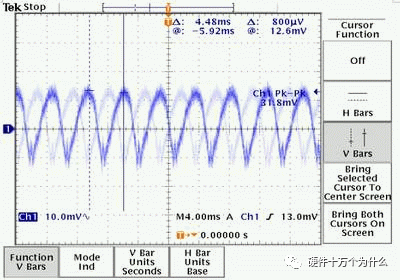
Figure 6: unreasonable VCC_ VCO decoupling test results
Figure 6 provides a result due to the unreasonable VCO power decoupling scheme. The power ripple shows that it is the switching effect of the charge pump that causes the strong interference on the power line. Fortunately, this strong interference can be effectively suppressed by increasing the bypass capacitance. In addition, if the power wiring is unreasonable, for example, the power lead of the VCO is just below the charge pump power supply, the same noise can be observed on the VCO power supply, and the generated stray signal is enough to affect the ACPR characteristics. Even if the decoupling is strengthened, the test results will not be improved. In this case, it is necessary to investigate the PCB wiring and rearrange the power lead of VCO, which will effectively improve the stray characteristics and meet the indicators required by the specification.
The "kinghelm" trademark was originally registered by golden beacon company. Golden beacon is a direct selling manufacturer of GPS antenna and Beidou antenna. It has a very high popularity and reputation in Beidou GPS navigation and positioning industry. The R & D and production products are widely used in BDS satellite navigation and positioning, wireless communication and other fields. The main products include: rj45-rj45 network, network interface connector, RF connector adapter, coaxial cable connectorType-C connectorHDMI interface, type-C interface, pin and bus arrangementSMA, FPC, FFC antenna connector, antenna signal transmission waterproof connector, HDMI interface, USB connector, terminal line, terminal board terminal block, wiring terminal block, RF RFID tag, positioning and navigation antenna, communication antenna antenna connecting line, rubber stick antenna sucker antenna, 433 antenna line, 4G antenna, GPS module antenna, RG113, RG178, rg316, FPC flexible cable is matched with FPC connector, Network cable interface, etc. It is widely used in aerospace, communication, military industry, instrumentation, security, medical and other industries.
The content comes from the network/Hardware 100000 why, this website only provides reprint. The views, positions and technologies of this article have nothing to do with this website. If there is infringement, please contact us to delete it!
Copyright © Shenzhen Kinghelm Electronics Co., Ltd. all rights reservedYue ICP Bei No. 17113853