Service hotline
+86 0755-83975897
 en
en Release date:2021-12-28Author source:KinghelmViews:2501
Internet of Things Chip Market Overview
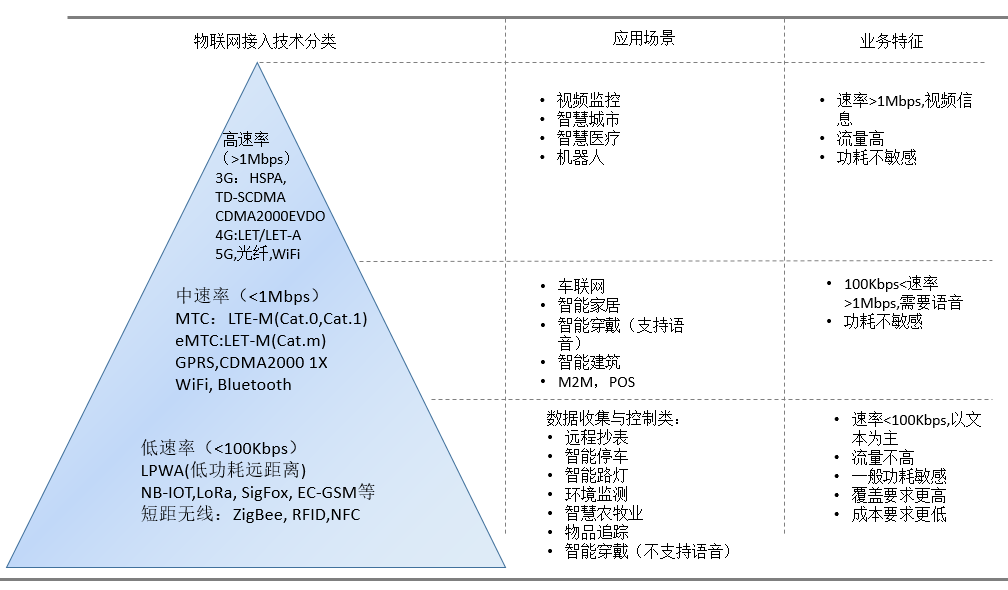
Internet of Things (IoT) has opened hundreds of billion Internet smart devices to communicate with each other. Only the total number of global networks has reached 12 billion in 2019. It is estimated that the total number of global network connections will reach 24.6 billion in 2025. my country's Internet of Things will also reach 801 billion. As of 2020, my country's Internet of Things industry has exceeded 1.7 trillion yuan. "Take" core "joint," core "accompanied" object %% The amount of compound annual growth rate is also expected to reach 13.3%.
Challenges in IoT Chip Design
1More working bands and higher work efficiency
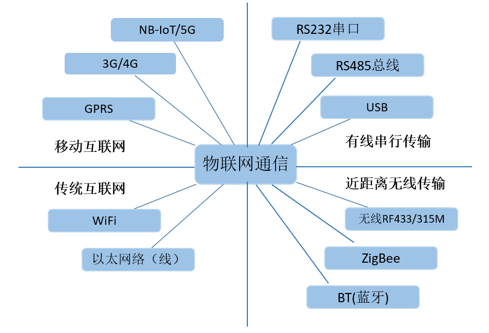
Compared with the communication chip in the traditional communication device is only responsible for connecting and transmitting signals, the application scenarios of the Internet of Things have obvious special features, covering wired and wireless communication modes, and wireless communication modules also involve from WiFi, BT (Bluetooth), ZigBee's short-range communication to NB-IOT, LTE Cat1, 5G and other Internet of Things, a wide variety of wireless communication types, involving frequency bands and frequency band combinations that need to be supported, also significantly increased, NB-IOT, 5G equal length distance The application of the communication network also brings a higher operating frequency requirements.
2 Complicated chip manufacturing process application scenario
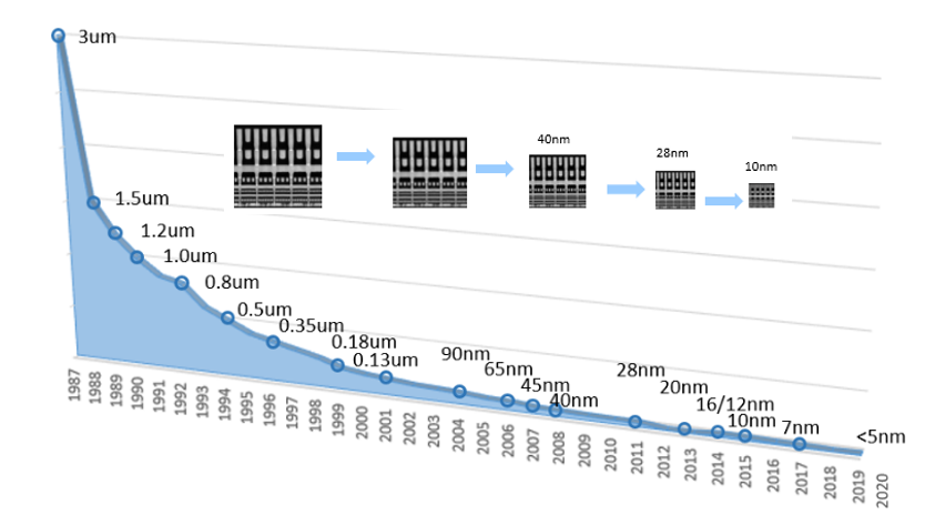
The advantages of various different chip manufacturing processes are needed in the IoT chip design, thereby increasing the performance of the circuit. Currently mainstream processes include CMOS, SOI and SiGe Bi-CMOS. Low-power CMOS processes are often the primary choice for circuit designers, and their process nodes are getting smaller in order to reduce costs.
3 Chip diversity and integration
The advantages of various different chip manufacturing processes are needed in the IoT chip design, thereby increasing the performance of the circuit. Currently mainstream processes include CMOS, SOI and SiGe Bi-CMOS. Low-power CMOS processes are often the primary choice for circuit designers, and their process nodes are getting smaller in order to reduce costs.
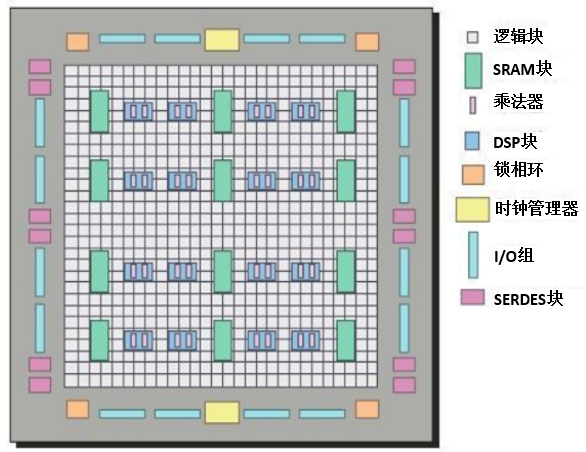
Core and IoT Chip Electromagnetic Simulation Solutions
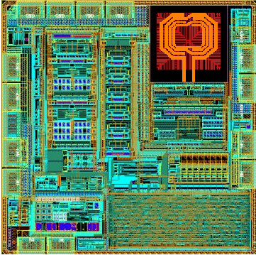
The solution we introduced in this article hopes to help the circuit designer for efficient passive structural simulation, modeling, extraction, and optimization for these modules.
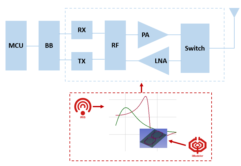
1 Passive structure multi-process angle quick extraction
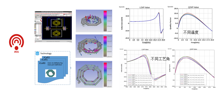
Strict certification. IRIS combines 3D full-wave solution technology to meet the extraction accuracy requirements from DC to millimeter bands. Users can flexibly create simulation unit modules, then use multi-thread / multi-core technology, MPI multi-machine processing technology will decompose complex simulation problem and improve simulation efficiency. IRIS software performs an integrated passive device simulation analysis to match the process angle and temperature scan module, which can quickly understand the characteristics of process status and device with process changes, and the circuit designer predicts the devices characteristic changes to the final circuit due to process deviations. The impact of performance has guiding significance.
2 Efficient modeling of passive devices
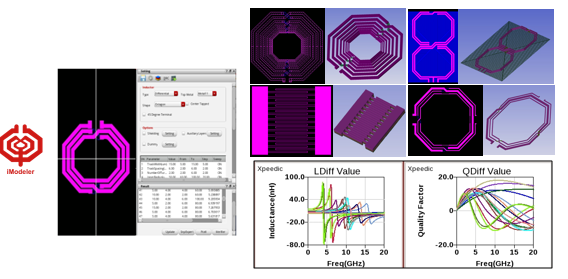
In addition, our solution also includes a passive device custom platform IMODELER based on a neural network algorithm. The user uses the inductors needed in this tool, and the transformers and other templates can quickly create PCell, and then quickly converge in the IRIS in IRIS in IRIS to get the passive device layout structure, You can also utilize multiple auxiliary options in the template to realize the forward and direction extraction of the passive device, which in turn can obtain devices that meet the circuit design requirements.
Summarize summary:
This article describes the features of the Internet of Things chip: more operating bands and higher operating frequencies, complex multi-chip manufacturing process application scenarios, chip diversity and integration, which brings new challenges to chip design . The core and semiconductor have launched a systemic Internet of Thine chip electromagnetic simulation solution: using Iris / Imodeler software to achieve fast and high-precision passive devices and interconnected electromagnetic emulation, passive device optimization modeling, etc. Application, greatly improves the design accuracy and design efficiency of circuit designers, and speeds up the product market.
"Kinghelm" trademark is registered by Jinhang standard company, Jinhang standard is a GPS antenna Beidou antenna R %& D to produce direct sales manufacturers, in the Beidou GPS navigation positioning industry very high popularity and reputation, research and development and production products are widely used in BDS satellite navigation positioning wireless communication, etc. field. The main products include: RJ45-RJ45 network, network interface connector, radio frequency connector switch, coaxial cable connector, TYPE-C connector, HDMI interface TYPE-C interface, pin roller, SMA, FPC, FFC Antenna connector, antenna signal transmission waterproof connector, HDMI interface, [敏感词]B connector, terminal terminal, terminal block terminal, terminal block, radio RFID tag, positioning navigation antenna, communication antenna antenna cable, glue rod antenna suction antenna, 433 Antenna 4G antenna, GPS module antenna, etc. Widely used in aerospace, communication, [敏感词], instrumentation and security, medical and other industries.
This content comes from network / xpeedic. This website only provides reprint, and the technical point of view is not related to this website. If there is any infringement, please contact us to delete!
Copyright © Shenzhen Kinghelm Electronics Co., Ltd. all rights reservedYue ICP Bei No. 17113853
