Service hotline
+86 0755-83975897

Release date:2023-06-10Author source:KinghelmViews:1756
WiFi antennas are devices used to receive and transmit wireless network signals. They can convert wireless signals into electrical signals or vice versa. Below is a brief introduction to the classification and application requirements of WiFi antennas:
一、Types and Forms of WiFi Antennas
1.On-Board Antennas
These antennas are directly formed with the circuit board, making them easy to mass-produce and cost-effective. However, their performance is limited and they are integrated into RF radio frequency modules. As shown in the figure below, a clear space of 20*5mm is generally required for the antenna, and it should be designed in the corner of the board without any metal coverage around it.

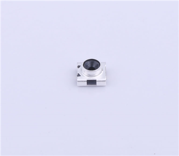
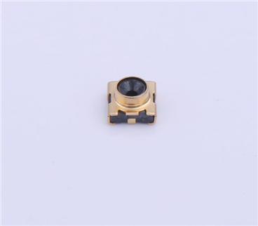
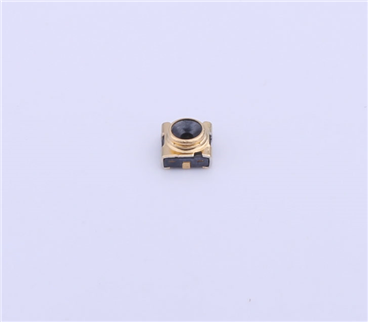
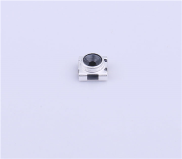
2.SMT Surface Mount Antennas
These antennas are made of materials such as ceramics, metal sheets, and PCBs. They have moderate performance and cost, and are suitable for mass-produced embedded RF modules. As shown in the figure below (ceramic patch antenna), they are directly mounted on the main board and have the characteristics of small size and easy mass production. The antenna size is 521mm, and the required space is 11*8mm. The best location for the antenna is in the corner of the board, and there should be no metal coverage above or below the antenna.

As shown in the figure below (metal sheet & PCB plug-in antenna), it is directly soldered onto the main board, with easy installation, high gain, and excellent performance. The antenna size is 20*7mm, and the PCB material thickness is 0.5~1mm. If the copper sheet antenna is a three-dimensional structure, the thickness is 3~5mm. The antenna should be designed in the corner of the board edge, and there should be no metal coverage above or below the antenna. There should be no components higher than 3mm within 10mm around the antenna.

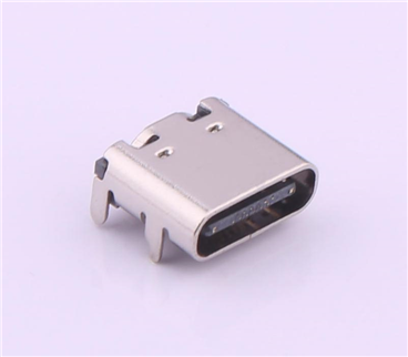
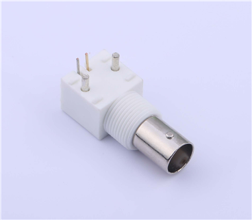
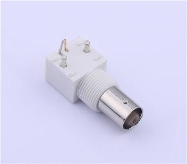
3.IPX External Antennas
These antennas use a combination of PCB or FPC+Cable, with high performance, high gain efficiency, wide application, moderate cost, and flexible installation. They can be fixed with adhesive or clips, and are usually installed inside the machine’s casing with adhesive. They are widely used in OTT and terminal equipment. As shown in the figure below, this type of antenna comes in various sizes and is suitable for projects with sufficient shell space and high performance requirements. Actual design needs to be matched and debugged according to the spatial structure and environment.

4.External Antennas
These are generally plastic rod-shaped antennas with high performance, independence, and high cost. They are used in terminal equipment.
二、Requirements of WiFi Antennas for PCB Layout and Structure
Antenna design largely depends on the characteristics of the installed platform, so it is a sensitive design for each platform. From the perspective of terminal hardware designers, how can we consider the impact on antennas when designing circuits and PCBs to increase the chances of project success? Here are some suggestions, but each project and device still needs to be analyzed specifically.
1.Suggestions for Antenna Form, Position, and Feed Point Size
The commonly used forms of built-in antennas are patch antennas, chip antennas, and FPC antennas. The form of the chip antenna is standardized, with fixed size and position of the solder pads according to the specific antenna specifications. In addition, there are design guidelines for the required clear space around the antenna and recommended device size for specific antenna models.
For patch antennas, it is recommended to use PIFA antennas as WiFi antennas. Based on experience, PIFA antennas have a higher success rate and better performance. The RF feed pad size of the antenna is 2~3mm, and the area around the pad should not have copper on all layers of the PCB. If it is a PIFA antenna, an additional 2~3mm ground pad should be added, with a distance of 2mm between the two pads.
The antenna is usually located on the top of the device, starting from the top of the PCB. Cut off the ground of all layers within this area by 2~3mm, but the solder pad of the layer that belongs to the antenna ground pad should be retained.
2.Suggestions for Matching Circuit Layout

The topology structure of the antenna matching circuit is four components in series and parallel from the antenna, leading to the test port or power amplifier. The area below the matching circuit and within 1.5mm around the matching network should not be grounded. It is better to place the matching network closer to the feeding solder pad (but not too close).
3.Microstrip Line from WiFi Module to Antenna Matching Circuit
The signal transmission line from the WiFi module to the antenna matching circuit is a microstrip line with a characteristic impedance of 50 ohms. To avoid losses on the microstrip line, the module should be placed as close as possible to the antenna. The dimensions of the microstrip line must be determined based on the specific PCB. Crossed lines between the microstrip line and ground are not allowed.
4.Grounding Issues
Good RF grounding is undoubtedly important for the wireless performance of the device, and the following design principles should be followed:
Try to keep the ground of the outer area intact and not divided or damaged (except for the part inside the shielding cover), which is particularly important for the area near the antenna. The antenna current must be isolated from the noise current. If the grounding area near the antenna is damaged and incomplete, a filling ground plane must be created in the relevant area and stitched with a ground via to make it a complete ground. The routing in this area must ensure that the antenna current only flows through the surface plane and limit the noise current from flowing into the complete ground plane inside.
When using pre-manufactured antennas, it should be noted that their characteristics depend on the connected ground plane. Only when the size and shape of the ground plane are consistent with the manufacturer’s evaluation board can the specifications indicated by the manufacturer be achieved. In other cases, users need to measure the impedance of the pre-manufactured antenna under actual application conditions and match it to the desired characteristic impedance.
5.Use of Metal Components in Device Enclosure
Do not use spray or coating with metal components on the surface of the enclosure. Metal coatings cannot achieve reliable grounding and will greatly affect antenna performance. Do not use metal decorations near the antenna.
6.Use of Pure Metal Structural Components
When using components with a full metal structure (such as front or rear panels), please reserve multiple grounding points for the components used. The specific grounding point location is determined by the antenna design company. There should be no grounded or ungrounded metal decorations, including plating and gold plating, above the antenna radiation area.
7.Considerations for Reserving Installation Space for Antennas
The antenna installation should be far away from metal objects, and the antenna needs enough space to unfold. If a chip antenna is used, a sufficient clearance area and corresponding size of the ground should be provided according to the application guide.
If a spring antenna is used, a support bracket should be designed for the antenna, and the antenna should be fixed on the bracket, and the bracket and PCB should be fixed; or the antenna should be fixed on the enclosure without a bracket.
When designing the structure, consider providing space and location for antenna installation, and consider adding hot-melt columns to the bracket or enclosure where the antenna is to be installed.
8.Considerations for Layout of Other Modules Relative to Antennas
For components such as speakers, cameras, vibrators, LCDs, and batteries, and their relative positions to the antenna, here are some common suggestions:
The antenna should be far away from the camera and flexible PCB;
The antenna should be at least 5mm away from the battery;
The vibrator should be far away from the antenna;
The distance from the antenna to the shielding cover should be a minimum of 2-4mm (which can cause parasitic effects);
RF switches and amplifiers or duplexers should be placed as close as possible to the matching circuit area.
Copyright © Shenzhen Kinghelm Electronics Co., Ltd. all rights reservedYue ICP Bei No. 17113853